GeOI (Ge-on-insulator) structure and preparation method
A composite and germanium layer technology, applied in semiconductor/solid-state device manufacturing, electrical components, circuits, etc., can solve the problems that the preparation method needs to be improved
- Summary
- Abstract
- Description
- Claims
- Application Information
AI Technical Summary
Problems solved by technology
Method used
Image

Examples
Embodiment 1
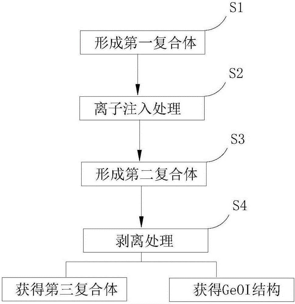
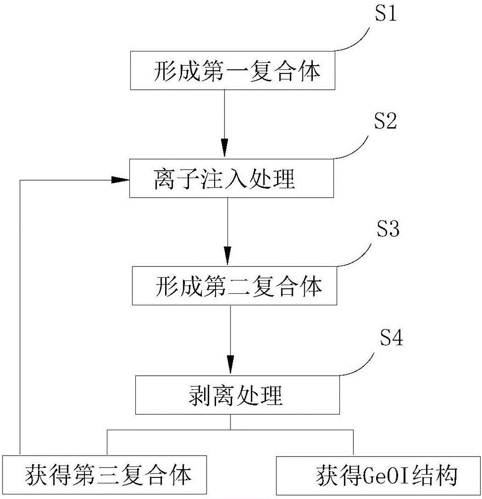
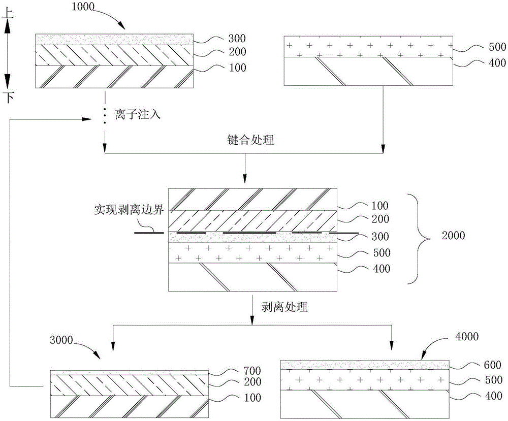
[0078] (1) Using reduced pressure chemical vapor deposition technology, SiH 4 and GeH 4 As a gas source, using a 12-inch silicon polished wafer as a substrate, first epitaxially form a germanium transition layer. During epitaxy, the substrate temperature is first 400 degrees Celsius for 30 minutes to form a Ge epitaxial seed layer with a thickness of about 30 nm and control the punching dislocation density. Raise the temperature to 750 degrees Celsius to form a germanium transition layer (the transition layer contains a Ge epitaxial seed layer) with a thickness of about 1.5 microns. Then in the same equipment, lower the temperature to 600 degrees Celsius to form a germanium layer of about 200nm. Then the temperature was raised to 825 degrees Celsius, and at the same time hydrogen was passed through for annealing for 120 minutes, so as to improve the smoothness of the germanium surface and facilitate subsequent bonding. In this way the first complex is obtained.
[0079] (2)...
Embodiment 2
[0083] (1) Using reduced pressure chemical vapor deposition technology, SiH 4 and GeH 4 As a gas source, using a 12-inch silicon polished wafer as the substrate, first epitaxially form a germanium transition layer. During epitaxy, the substrate temperature is first 400 degrees Celsius for 30 minutes to form a Ge epitaxial seed layer with a thickness of about 30nm and control the punching dislocation density. Raise the temperature to 750 degrees Celsius to form a germanium transition layer (the transition layer contains a Ge epitaxial seed layer) with a thickness of about 1.5 microns. The temperature is raised to 825 degrees Celsius, and at the same time hydrogen is passed through for annealing for 120 minutes, so as to improve the smoothness of the surface of the germanium transition layer, which is beneficial to the subsequent bonding. In the same equipment, the temperature is lowered to 500 degrees Celsius to form 20nm thick Si 0.3 Ge 0.7 strain layer. Then, in the same ...
Embodiment 3
[0088] (1) Using reduced pressure chemical vapor deposition technology, SiH 4 and GeH 4 As a gas source, using a 12-inch silicon polished wafer as the substrate, first epitaxially form a germanium transition layer. During epitaxy, the substrate temperature is first 400 degrees Celsius for 30 minutes to form a Ge epitaxial seed layer with a thickness of about 30nm and control the punching dislocation density. Raise the temperature to 750 degrees Celsius to form a germanium transition layer (the transition layer contains a Ge epitaxial seed layer) with a thickness of about 1.5 microns. The temperature is raised to 825 degrees Celsius, and at the same time hydrogen is passed through for annealing for 120 minutes, so as to improve the smoothness of the surface of the germanium transition layer, which is beneficial to the subsequent bonding. In the same equipment, the temperature is lowered to 500 degrees Celsius to form 20nm thick Si 0.3 Ge 0.7 strain layer. In the same equipm...
PUM
 Abstract
Description
Claims
Application Information
 - R&D
- Intellectual Property
- Life Sciences
- Materials
- Tech Scout
- Unparalleled Data Quality
- Higher Quality Content
- 60% Fewer Hallucinations
Browse by: Latest US Patents, China's latest patents, Technical Efficacy Thesaurus, Application Domain, Technology Topic, Popular Technical Reports.
© 2025 PatSnap. All rights reserved.Legal|Privacy policy|Modern Slavery Act Transparency Statement|Sitemap|About US| Contact US: help@patsnap.com