
Method for achieving enhanced HEMT through polarity control and enhanced HEMT

A polarity control and enhancement technology, applied in the field of microelectronics technology, can solve the problem of device performance degradation, and achieve the effects of high repeatability, easy mass production and low cost

Inactive Publication Date: 2017-03-22
SUZHOU INST OF NANO TECH & NANO BIONICS CHINESE ACEDEMY OF SCI
View PDF3 Cites 10 Cited by
  • Summary
  • Abstract
  • Description
  • Claims
  • Application Information

AI Technical Summary

Problems solved by technology

For another example, F plasma treatment can also realize enhanced HEMT devices, and does not require etching, but F plasma will also etch the barrier layer during the implantation process, resulting in a decrease in device performance

Method used

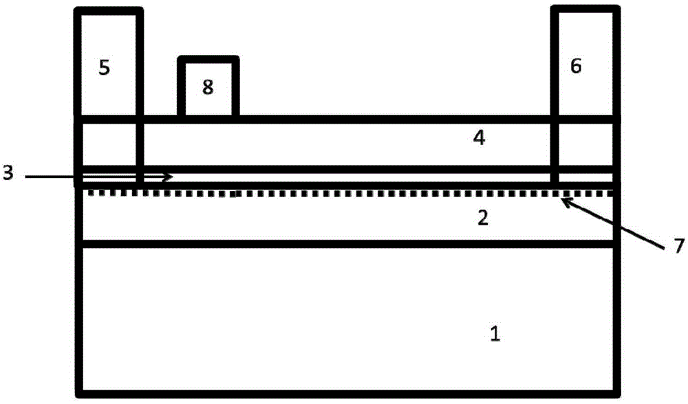
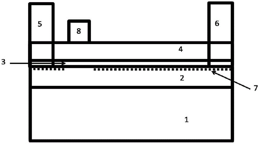
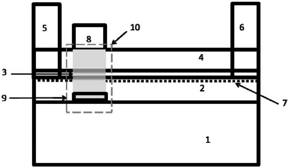

Image

  • Method for achieving enhanced HEMT through polarity control and enhanced HEMT
  • Method for achieving enhanced HEMT through polarity control and enhanced HEMT
  • Method for achieving enhanced HEMT through polarity control and enhanced HEMT

Examples


Embodiment Construction

[0019] The technical solution of the present invention will be explained in more detail below. However, it should be understood that within the scope of the present invention, the above-mentioned technical features of the present invention and the technical features specifically described in the following (such as embodiments) can be combined with each other to form new or preferred technical solutions. Due to space limitations, we will not repeat them here.

[0020] One aspect of the invention relates to an enhanced HEMT. In some embodiments, the enhanced HEMT includes: a heterostructure mainly composed of a first semiconductor layer serving as a channel layer and a second semiconductor layer serving as a barrier layer, and a Source, drain, and gate electrodes; the source and drain electrodes are electrically connected through two-dimensional electrons formed in the heterostructure, and the gate electrode is distributed between the source and drain electrodes. Wherein, the ...


PUM


Abstract

The invention discloses an enhanced HEMT, which comprises a heterostructure, a source electrode, a drain electrode and a gate electrode, wherein the heterostructure mainly comprises a first semiconductor layer and a second semiconductor layer; the source electrode, the drain electrode and the gate electrode are connected with the heterostructure; the source electrode and the drain electrode are electrically connected through a two-dimensional electron gas formed in the heterostructure; the gate electrode is distributed between the source electrode and the drain electrode; and component materials distributed in local areas of the first semiconductor layer and the second semiconductor layer below the gate electrode have set polarity, so that accumulation of the two-dimensional electron gas in the local area of the heterostructure below the gate electrode is avoided when zero bias is applied to the gate electrode or no bias is applied to the gate electrode, and the two-dimensional electron gas can be formed in the local area of the heterostructure below the gate electrode when voltage of the gate electrode is greater than threshold voltage. The invention further discloses a method for achieving the enhanced HEMT through polarity control. The method has the advantages of being simple in process and high in repeatability, the performance of a device is stable and excellent, the cost is low and large-scale production is easy to implement.

Description

technical field [0001] The present invention relates to an enhanced HEMT (high electron mobility transistor) device and a preparation method thereof, in particular to a method for realizing an enhanced HEMT device by adjusting the polarity of a semiconductor material grown under a gate electrode and utilizing a change in a polarization electric field , belonging to the field of microelectronic technology. Background technique [0002] HEMT devices are made by making full use of the two-dimensional electron gas formed by the semiconductor heterostructure (Heterostructure) structure. Compared with III-VI (such as AlGaAs / GaAs HEMT), III-nitride semiconductors are due to piezoelectric polarization And the spontaneous polarization effect, a high-concentration two-dimensional electron gas can be formed in the heterostructure (such as AlGaN / GaN). Therefore, in HEMT devices made of group III nitrides, the barrier layer generally does not need to be doped. At the same time, group I...

Claims


Application Information

Patent Timeline
Patent Type & Authority Applications(China)
IPC IPC(8): H01L29/778H01L29/20H01L21/335
CPCH01L29/7787H01L29/2003H01L29/66431
Inventor 张志利蔡勇张宝顺付凯于国浩孙世闯宋亮邓旭光
Owner SUZHOU INST OF NANO TECH & NANO BIONICS CHINESE ACEDEMY OF SCI
Learn More