Preparation method of mica thin film and transistor

A technology of transistors and mica, which is applied in the preparation method of mica thin films and the field of transistors, can solve the problems of deterioration of key performances such as breakdown voltage, efficiency, and gain of devices, affect the stability and reliability of device performance, and cannot completely prevent the impact, etc., to achieve The effect of suppressing current collapse, reducing process complexity, and reducing gate current

Active Publication Date: 2019-12-06
SUZHOU INST OF NANO TECH & NANO BIONICS CHINESE ACEDEMY OF SCI
View PDF3 Cites 0 Cited by
  • Summary
  • Abstract
  • Description
  • Claims
  • Application Information

AI Technical Summary

Problems solved by technology

However, this method is complicated in process, and it only reduces the current collapse to a certain extent, and cannot completely prevent the influence of the surface state on the two-dimensional electron gas in the main channel. When the electric field is high, the two-dimensional electron gas will still be captured by the surface state, thus affecting the device. Stability and reliability of performance
[0004] In addition, due to the large reverse leakage of Schottky gate AlGaN / GaN heterojunction devices, it will lead to the deterioration of key performances such as breakdown voltage, efficiency, and gain of the device.

Method used


Image

  • Preparation method of mica thin film and transistor
  • Preparation method of mica thin film and transistor

Examples


Embodiment Construction

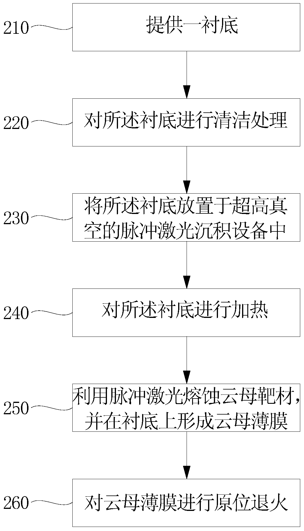
[0018] In order to better illustrate the technical means adopted by the present invention and its effects, a detailed description will be given below in conjunction with the embodiments of the present invention and the accompanying drawings. It will, however, be evident that various changes and modifications can be made to the present invention without departing from the broader spirit and scope of the invention as defined in the appended claims. Therefore, the following examples have an illustrative rather than a limiting meaning.

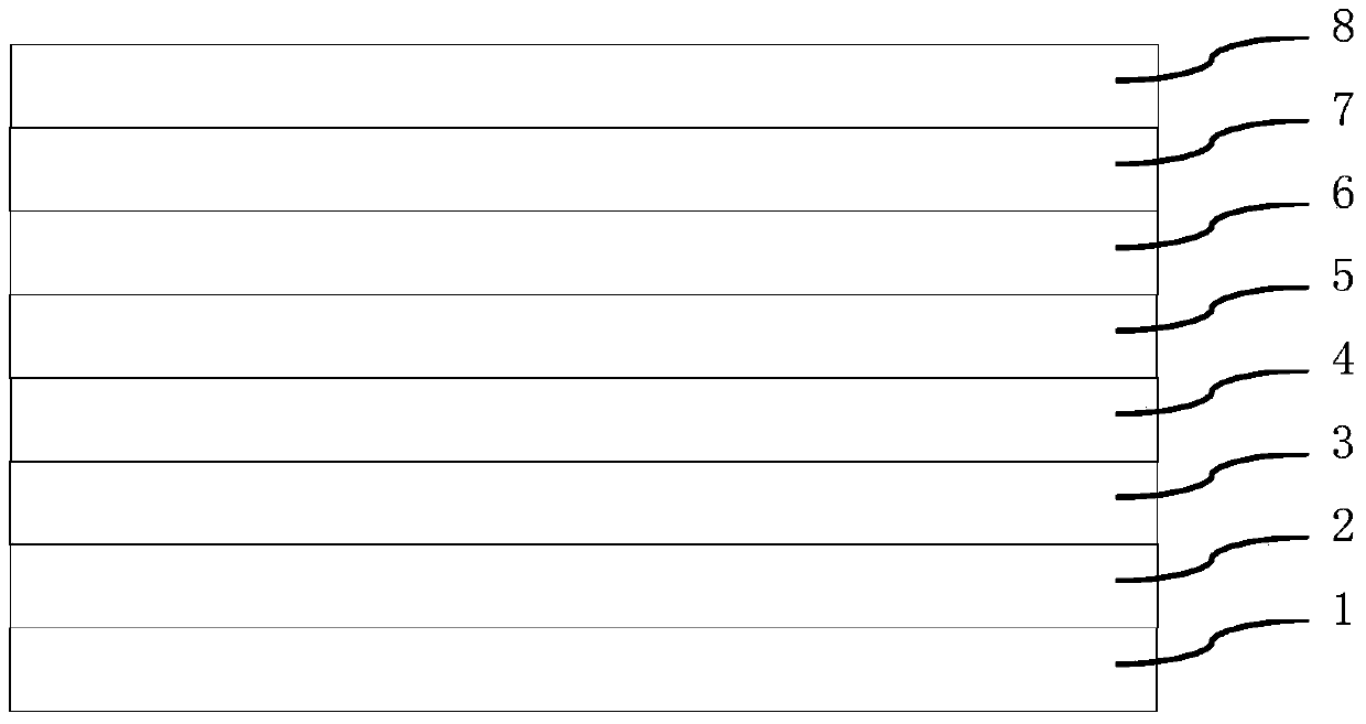
[0019] figure 1 is a schematic diagram of a GaN-based high electron mobility transistor according to an embodiment of the present invention.

[0020] refer to figure 1 As shown, the gallium nitride-based high electron mobility transistor according to the embodiment of the present invention includes a substrate 1, a buffer layer 2 on the substrate 1, a gallium nitride high resistance layer 3 on the buffer layer 2, a nitrogen The gallium nitride ...


PUM

PropertyMeasurementUnit
thicknessaaaaaaaaaa
thicknessaaaaaaaaaa
thicknessaaaaaaaaaa

Abstract

The invention discloses a method for preparing a mica thin film, which comprises: placing a substrate in a vacuum pulsed laser deposition device; using a pulsed laser to ablate a mica target to generate a plasma plume on the surface of the mica target, the resulting The plasma plume is deposited on the substrate to form a uniform mica film. The invention also discloses a transistor, which includes the mica film prepared by the preparation method. The transistor of the present invention introduces the mica thin film as the dielectric layer, and because the layered two-dimensional nanostructure of the mica has an ultra-thin thickness, it is beneficial to gate modulation of the transistor and high-density integration of the transistor in the vertical direction. In addition, the surface of the mica film is very smooth, which makes the carriers of the transistor free from the influence of surface roughness and trap states, so that the transistor can obtain higher carrier mobility.

Description

technical field [0001] The invention relates to the technical field of thin film preparation, in particular to a method for preparing a mica thin film and a transistor. Background technique [0002] As a typical representative of wide-bandgap semiconductor materials, gallium nitride (GaN)-based materials have the characteristics of large bandgap width, high electron saturation drift velocity, high breakdown field strength, and good thermal conductivity. They can be used to make high-temperature, high-frequency and high power electronics. More importantly, GaN-based materials can form modulation-doped AlGaN / GaN heterostructures, which can obtain high electron mobility, extremely high peak electron velocity and saturation electron velocity at room temperature, and obtain better than the first Higher two-dimensional electron gas density in second-generation compound semiconductor heterostructures. Therefore, high electron mobility transistors based on AlGaN / GaN heterojunction...

Claims


Application Information

Patent Timeline
Patent Type & Authority Patents(China)
IPC IPC(8): H01L21/314H01L29/778
CPCH01L21/02145H01L21/02161H01L21/02266H01L29/778
Inventor 高雪刘建平孙钱张书明杨辉
Owner SUZHOU INST OF NANO TECH & NANO BIONICS CHINESE ACEDEMY OF SCI
Why Eureka
Try Eureka