Semiconductor device, preparation method thereof and electronic device

A technology for electronic devices and semiconductors, applied in semiconductor devices, semiconductor/solid-state device manufacturing, circuits, etc., and can solve problems such as multiple ion implantation

Active Publication Date: 2017-04-26
SEMICON MFG INT (SHANGHAI) CORP +1
View PDF4 Cites 2 Cited by
  • Summary
  • Abstract
  • Description
  • Claims
  • Application Information

AI Technical Summary

Problems solved by technology

[0006] Solid source-drain doping methods can be used to dope the bottom of the channel, by which both up-diffusion into the channel and ion implantation damage can be well controlled, but there are other problems with this method, among them, FinFET devices usually include a core area a

Method used


Image

  • Semiconductor device, preparation method thereof and electronic device
  • Semiconductor device, preparation method thereof and electronic device
  • Semiconductor device, preparation method thereof and electronic device

Examples


Embodiment 1

[0061] In order to solve the problems in the prior art, the present invention provides a new method for manufacturing a semiconductor device. The method of the present invention will be further described below in conjunction with the accompanying drawings.

[0062] in, Figure 1-13 It is a schematic diagram of the manufacturing process of the semiconductor device described in a specific implementation of the present invention.

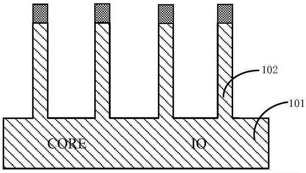
[0063] First, step 101 is performed to provide a semiconductor substrate 101 .

[0064] Specifically, such as figure 1 As shown, in this step, the semiconductor substrate can be at least one of the materials mentioned below: silicon, silicon-on-insulator (SOI), silicon-on-insulator (SSOI), silicon-germanium-on-insulator ( S-SiGeOI), silicon germanium on insulator (SiGeOI) and germanium on insulator (GeOI), etc.

[0065] In this embodiment, silicon is selected as the semiconductor substrate 101 .

[0066] Wherein the semiconductor substrate includes...

Embodiment 2

[0117] The present invention also provides a semiconductor device, which is prepared by the method described in the first embodiment.

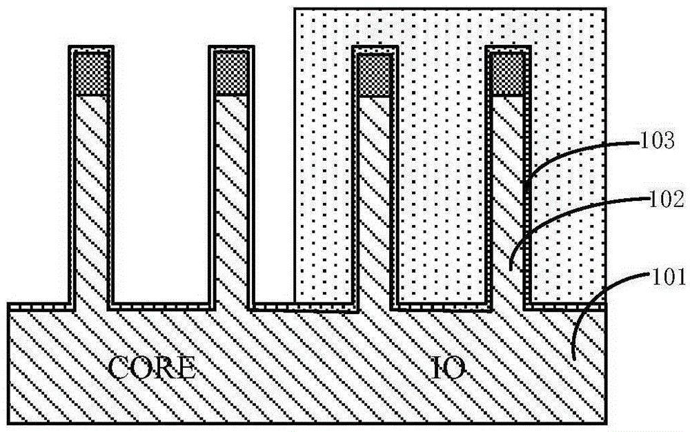
[0118] A semiconductor substrate 101, the semiconductor substrate includes a core area and an input and output area;

[0119] Fins 102 located on the core area and the input and output areas;

[0120] an isolation material layer 106 located on the semiconductor substrate and covering part of the fins;

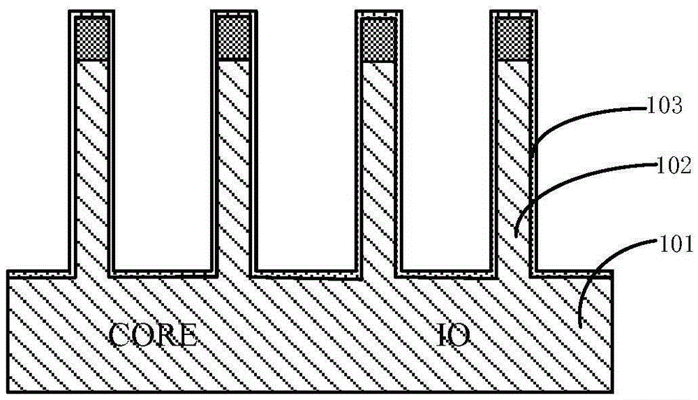
[0121] Wherein, a boron-containing material layer 104 and a covering layer 105 are sequentially formed on the surface of the part of the fin covered by the isolation material layer 106, wherein, in the input-output region, the fin and the boron-containing A liner layer 103 is also formed between the material layers 104 .

[0122] Wherein, the semiconductor substrate 101 may be at least one of the materials mentioned below: silicon, silicon-on-insulator (SOI), silicon-on-insulator (SSOI), silicon-germanium-on-insulator (S-SiGeOI) , silicon ge...

Embodiment 3

[0134] The present invention also provides an electronic device, including the semiconductor device described in the second embodiment. Wherein, the semiconductor device is the semiconductor device described in the second embodiment, or the semiconductor device obtained according to the preparation method described in the first embodiment.

[0135] The electronic device of this embodiment can be any electronic product or equipment such as mobile phone, tablet computer, notebook computer, netbook, game console, TV set, VCD, DVD, navigator, camera, video recorder, voice recorder, MP3, MP4, PSP, etc. , can also be any intermediate product including the semiconductor device. The electronic device according to the embodiment of the present invention has better performance due to the use of the above-mentioned semiconductor device.


PUM


Abstract

The invention relates to a semiconductor device, a preparation method thereof and an electronic device. The method comprises the steps of (S1) providing a semiconductor substrate which comprises a core area and an input and output area, wherein a plurality of fins is formed in the core area and the input and output area, (S2) forming liner layers on the semiconductor substrate of the input and output area and the side walls of the bottoms of the fins, (S3) orderly forming a boron-containing material layer and a covering layer on the semiconductor substrate of the core area, the surfaces of the fins, the linear layer in the input and output area and the surfaces of the tops of the fins, (S4) forming an isolation material layer on the covering layer to the top of the linear layer or higher so as to partly cover the fins, and (S5) removing the boron-containing material layer and the covering layer on exposed fins, and (S6) executing annealing such that the boron in the boron-containing material layer is diffused to a channel stop area.

Description

technical field [0001] The present invention relates to the field of semiconductors, in particular, the present invention relates to a semiconductor device, a preparation method thereof, and an electronic device. Background technique [0002] The improvement of integrated circuit performance is mainly achieved by continuously shrinking the size of integrated circuit devices to increase its speed. Currently, as the semiconductor industry has advanced to nanotechnology process nodes, especially as semiconductor device dimensions drop to 22nm or below, manufacturing and design challenges have prompted the development of three-dimensional designs such as Fin Field Effect Transistors (FinFETs). [0003] Compared with the existing planar transistors, the FinFET device has more superior performance in terms of channel control and reducing shallow channel effects; the planar gate structure is arranged above the channel, and the gate in the FinFET The fins are arranged around the fi...

Claims


Application Information

Patent Timeline
IPC IPC(8): H01L21/336H01L29/78H01L29/06
CPCH01L29/06H01L29/66795H01L29/785H01L21/823431H01L21/823821H01L29/66803
Inventor 周飞
Owner SEMICON MFG INT (SHANGHAI) CORP
Why Eureka
Try Eureka