Thin film transistor and its preparation method, array substrate

A technology of thin film transistors and substrates, which is applied in the fields of transistors, semiconductor/solid-state device manufacturing, semiconductor devices, etc., can solve the problems of increasing process complexity, reducing production efficiency, and low production efficiency, and achieves performance improvement, suppression of leakage current, high The effect of on/off ratio

Active Publication Date: 2020-08-14
TRULY HUIZHOU SMART DISPLAY
View PDF5 Cites 0 Cited by
  • Summary
  • Abstract
  • Description
  • Claims
  • Application Information

AI Technical Summary

Problems solved by technology

However, this method requires expensive ion implantation equipment, low production efficiency, and high production costs
In addition, the lattice damage caused by ion implantation needs to be eliminated by high temperature annealing, which increases the complexity of the process and reduces the production efficiency

Method used


Image

  • Thin film transistor and its preparation method, array substrate
  • Thin film transistor and its preparation method, array substrate
  • Thin film transistor and its preparation method, array substrate

Examples


Embodiment Construction

[0032] In order to make the object, technical solution and advantages of the present invention clearer, the present invention will be further described in detail below in conjunction with the accompanying drawings and embodiments. It should be understood that the specific embodiments described here are only used to explain the present invention, not to limit the present invention.

[0033] In the description of the present invention, it should be understood that the terms "first" and "second" are used for description purposes only, and cannot be interpreted as indicating or implying relative importance or implicitly indicating the quantity of indicated technical features. Thus, the features defined as "first" and "second" may explicitly or implicitly include at least one of these features. In the description of the present invention, "plurality" means at least two, such as two, three, etc., unless otherwise specifically defined.

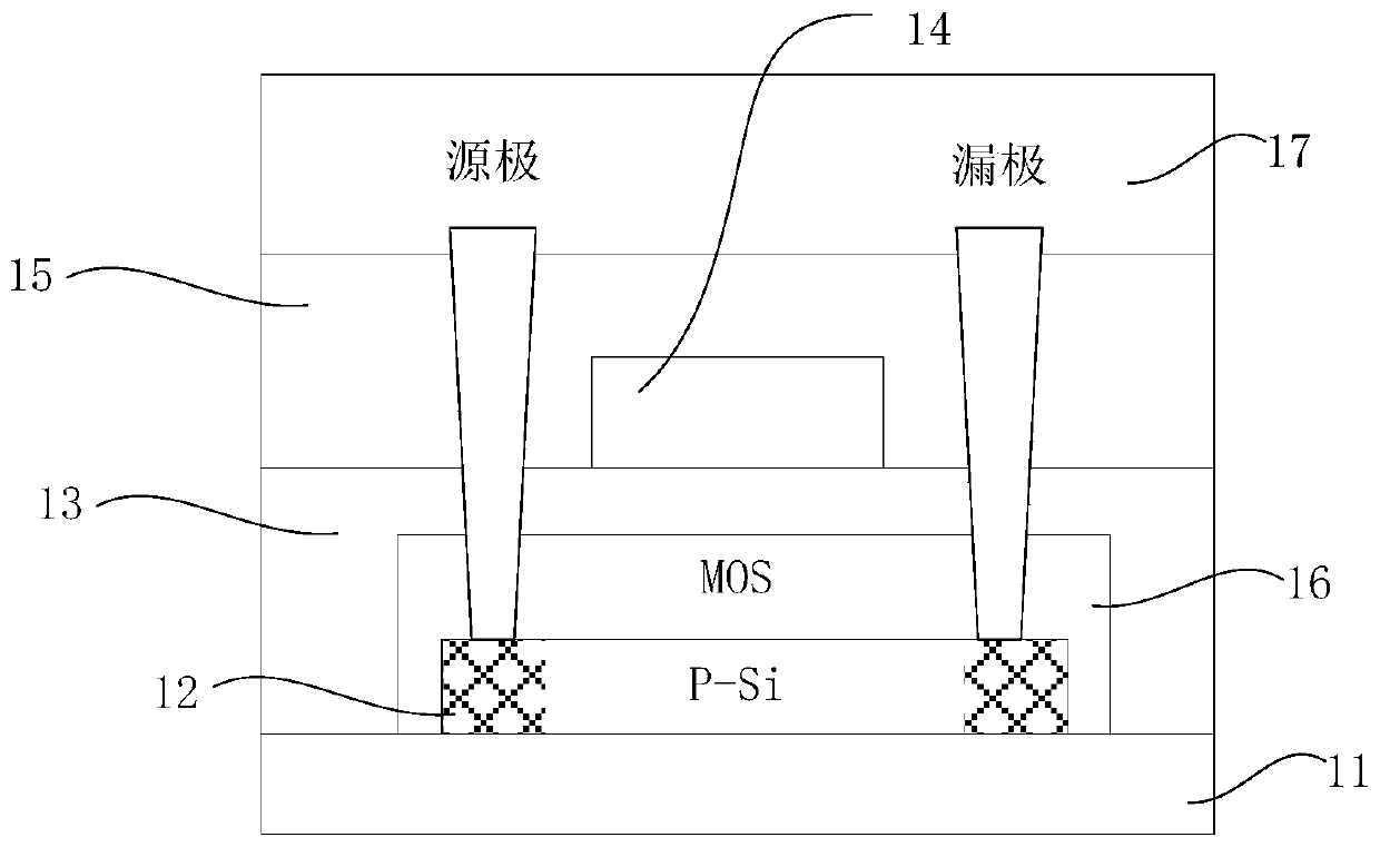
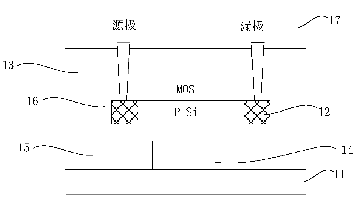
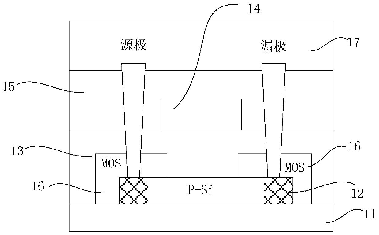
[0034] A thin film transistor, a manufacturin...


PUM

PropertyMeasurementUnit
thicknessaaaaaaaaaa
thicknessaaaaaaaaaa
thicknessaaaaaaaaaa

Abstract

The invention proposes a thin film transistor and preparation method thereof, and array substrate. The thin film transistor includes a substrate, an active layer, a gate insulating layer, a gate electrode, an interlayer insulating layer and source and drain electrodes, and is characterized in that the thin film transistor also includes at least one metal oxide semiconductor layer arranged on the active layer. According to the abovementioned thin film transistor and preparation method thereof, and the array substrate, through introduction of a metal oxide semiconductor, a weak inversion heterojunction is built in the vertical direction of the transistor, characteristics of longitudinal heterojunction weak inversion are introduced into a narrow-band high-resistance region in the horizontal direction, the depletion characteristic of a junction field effect transistor is avoided, and the purposes of suppressing leakage current and adjusting threshold voltage are achieved. At the same time, the characteristic of longitudinal heterojunction inversion charge accumulation shows a large current characteristic in the horizontal direction, and a high switch ratio is realized, thereby realizing improvement of an N channel thin film transistor in performance.

Description

technical field [0001] The present invention relates to the field of display technology, in particular to a thin film transistor, a preparation method thereof, and an array substrate including the thin film transistor. Background technique [0002] LTPS (Low Temperature Poly-silicon, low-temperature polysilicon) technology is a technology that projects laser light on a glass substrate with an amorphous silicon structure, so that the glass substrate with an amorphous silicon structure absorbs laser energy and transforms it into a polysilicon structure. Due to the low density of defect states and high carrier mobility (50-300cm 2 / VS), displays with low-temperature polysilicon thin films as electronic components show the advantages of high resolution, fast response, high brightness and high aperture ratio, so LTPS technology is currently widely used in display technology. [0003] Among them, transistors based on LTPS technology are prone to generate hot carriers, and the int...

Claims


Application Information

Patent Timeline
Patent Type & Authority Patents(China)
IPC IPC(8): H01L29/06H01L29/22H01L29/24H01L29/786H01L21/336
CPCH01L29/0688H01L29/22H01L29/24H01L29/6675H01L29/78672
Inventor 田金鹏张毅先任思雨苏君海李建华
Owner TRULY HUIZHOU SMART DISPLAY
Why Eureka
Try Eureka