Ring-gate structure field effect transistor and preparation method thereof

A technology of structure field and transistor, which is applied in semiconductor/solid-state device manufacturing, semiconductor devices, electrical components, etc., can solve problems such as the influence of semiconductor working performance, and achieve the effect of size reduction and good insulation properties

Inactive Publication Date: 2017-04-26
SHENZHEN UNIV
View PDF3 Cites 3 Cited by
  • Summary
  • Abstract
  • Description
  • Claims
  • Application Information

AI Technical Summary

Problems solved by technology

[0004] The technical problem to be solved by the present invention is to provide a field-effect transistor with a gate-all-around structure and its preparation method, which aim

Method used


Image

  • Ring-gate structure field effect transistor and preparation method thereof
  • Ring-gate structure field effect transistor and preparation method thereof
  • Ring-gate structure field effect transistor and preparation method thereof

Examples


preparation example Construction

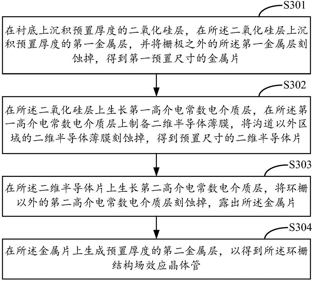
[0034] The present invention also provides image 3 A method for preparing a field effect transistor with a gate-all-around structure shown, comprising:

[0035] S301, depositing a silicon dioxide layer with a preset thickness on the substrate, depositing a first metal layer with a preset thickness on the silicon dioxide layer, and etching away the first metal layer except the gate , to obtain a metal sheet of the first preset size;

[0036] S302, growing a first high-permittivity dielectric layer on the silicon dioxide layer, preparing a two-dimensional semiconductor film on the first high-permittivity dielectric layer, and etching the two-dimensional semiconductor film in areas other than the channel Get a two-dimensional semiconductor chip with a preset size;

[0037] S303, growing a second high-permittivity dielectric layer on the two-dimensional semiconductor sheet, and etching away the second high-permittivity dielectric layer except the ring gate, exposing the metal s...


PUM

PropertyMeasurementUnit
Thicknessaaaaaaaaaa

Abstract

The invention is suitable for a semiconductor device and provides a ring-gate structure field effect transistor, which comprises a substrate, a silicon dioxide layer deposited on the substrate, and grid, source and drain electrodes deposited on the silicon dioxide layer. The grid electrode comprises an active layer, an insulation layer wrapping around the active layer and a metal layer wrapping around the insulation layer, wherein the insulation layer is made of a high-dielectric-constant dielectric material. The ring-gate structure field effect transistor, by adopting the high-dielectric-constant dielectric material to serve as the insulation layer, has a good insulation property, can produce a higher field effect between the grid electrode and a substrate channel, can reduce transistor electric leakage amount and reduce device power consumption and heating, and enables the size of the transistor to be further reduced.

Description

technical field [0001] The invention belongs to the field of semiconductor design, and in particular relates to a gate-around structure field effect transistor and a preparation method thereof. Background technique [0002] Early integrated circuits were basically based on the traditional planar transistor structure. The so-called planar transistor refers to a transistor whose source, drain, gate and channel cross-sections are on the same plane. . Although the development of planar transistor technology has been quite mature so far, and the cost has become increasingly low, but as the feature size of semiconductor devices is proportionally reduced according to Moore's law, the chip integration level continues to increase, and the short channel effect has a serious impact on performance, especially the feature size. The shrinkage leads to a significant increase in the channel effect, resulting in a sharp increase in the off-state current of the device. [0003] In order to ...

Claims


Application Information

Patent Timeline
IPC IPC(8): H01L29/78H01L29/423H01L21/336
CPCH01L29/4232H01L29/42356H01L29/42364H01L29/66477H01L29/7827
Inventor 何佳铸刘新科李奎龙陈乐何祝兵俞文杰吕有明韩舜曹培江柳文军曾玉祥贾芳朱德亮洪家伟
Owner SHENZHEN UNIV
Why Eureka
Try Eureka