
Silicon wafer surface passivation technique

A silicon wafer surface and silicon wafer technology, applied in the field of photovoltaic solar cells, can solve the problems of high cost, complicated operation, poor passivation effect, etc., and achieve the effects of easy operation, simple process and easy realization.

Inactive Publication Date: 2017-04-26
HEBEI UNIVERSITY
View PDF3 Cites 2 Cited by
  • Summary
  • Abstract
  • Description
  • Claims
  • Application Information

AI Technical Summary

Problems solved by technology

[0005] In addition, if only the minority carrier lifetime of silicon wafers is tested to provide data for the detection and screening of silicon materials, the above-mentioned high-temperature vacuum and other technologies are not applicable due to problems such as high cost and complicated operation.
Commonly used is passivation by soaking in hydrofluoric acid and iodine. The important disadvantage of this technology is that the passivation effect is poor. Minority lifetimes are typically below 1 millisecond

Method used


Image

  • Silicon wafer surface passivation technique
  • Silicon wafer surface passivation technique

Examples


Embodiment Construction

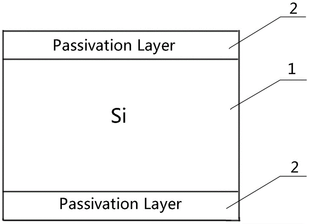
[0020] Such as figure 1 As shown, a passivation layer 2 is prepared on both the front surface and the back surface of the silicon wafer 1. The passivation layer 2 is a PSS film, and the PSS film can passivate the surface of the silicon wafer 1 very well. The thickness of the PSS thin film is on the order of nanometers. Preferably, the thickness of the PSS thin film is 30nm-1000nm. figure 1 What is shown in is just a specific example, and in other embodiments, the PSS film can also be formed on only one surface of the silicon wafer as a passivation layer. When the formed PSS film is used as a passivation layer, the passivation layer can fully cover the surface of the silicon wafer, or partially cover the surface of the silicon wafer, that is, the PSS film can be in partial contact with the surface of the silicon wafer, for example: to prepare a gate type The structured PSS film acts as a passivation layer.

[0021] The PSS thin film formed on the surface of the silicon wafer ...


PUM

PropertyMeasurementUnit
Thicknessaaaaaaaaaa

Abstract

The invention provides a silicon wafer surface passivation technique. By preparing a polystyrene sulfonic acid film on the surface of a silicon wafer, passivation of the surface of the silicon wafer is realized; the thickness of the polystyrene sulfonic acid film prepared on the silicon wafer is in a nanometer scale; after passivation of the surface of the silicon wafer through the polystyrene sulfonic acid film, a high-quality passivation effect can be obtained, and minority carrier lifetime can reach more than 20 ms; and besides, preparation of the polystyrene sulfonic acid film can be realized through a spin-coating method, a spraying coating method or a printing method and the like, and the passivation technique is simple in process, does not need vacuum or high temperature, and is safe and convenient to operate. The passivation technique has a very important application value for silicon material detection and silicon solar energy cell surface passivation.

Description

technical field [0001] The invention relates to the field of photovoltaic solar cells, in particular to a surface passivation technology for silicon wafers. Background technique [0002] The interior of the silicon material is a very neat and orderly arrangement of atoms, and the lattice is periodic. Carriers have good migration and transport capabilities inside it. But on the surface of the silicon wafer, due to the periodic interruption of the crystal lattice, a large number of dangling bonds are generated, and these dangling bonds become the recombination centers of carriers, that is, surface recombination. Surface recombination is fatal to solar cells, and strong surface recombination directly leads to extremely poor performance of silicon solar cells. The effect of surface recombination is also very important in the microelectronics industry, such as thin-film silicon transistors, and the interface defect states at the drain have a very important impact on device perf...

Claims


Application Information

Patent Timeline
IPC IPC(8): H01L31/18
CPCH01L31/1804H01L31/1868Y02E10/547Y02P70/50
Inventor 麦耀华沈艳娇陈兵兵郭建新许颖陈剑辉
Owner HEBEI UNIVERSITY
Features
  • Generate Ideas
  • Intellectual Property
  • Life Sciences
  • Materials
  • Tech Scout
  • Unparalleled Data Quality
  • Higher Quality Content
  • 60% Fewer Hallucinations
Learn More