

Infrared detector with microbridge structure and production method thereof
An infrared detector and micro-bridge structure technology, applied in the field of infrared detectors, can solve the problems of complex surface structure of the infrared absorption layer, failure of the thermal insulation of the micro-bridge, and reduced yield, etc., so as to avoid the contact between the suspended part and the micro-bridge structure, The effect of reducing difficulty, improving performance and yield
- Summary
- Abstract
- Description
- Claims
- Application Information
AI Technical Summary
Problems solved by technology
Method used
Image

Examples
Embodiment Construction
[0026] The specific implementation of the infrared detector with micro-bridge structure and its manufacturing method provided by the present invention will be described in detail below with reference to the accompanying drawings.
[0027] Please refer to figure 1 , is a flow chart of a method for manufacturing an infrared detector with a microbridge structure according to a specific embodiment of the present invention.
[0028] The manufacturing method of described infrared detector comprises:
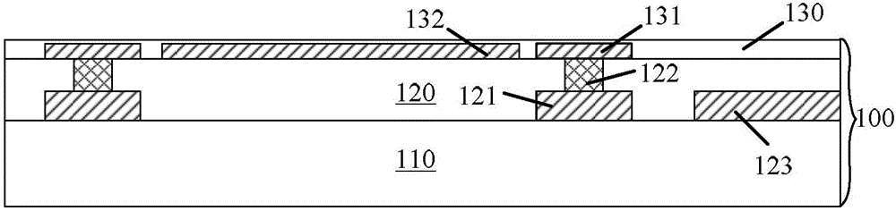
[0029] Step S101: providing a substrate, a metal interconnection layer is formed in the surface of the substrate.
[0030] Step S102: forming a first sacrificial layer on the surface of the substrate, the first sacrificial layer having a first through hole located on the surface of the metal interconnection layer.
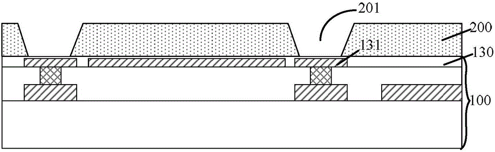
[0031] Step S103: forming a patterned micro-bridge structure on the inner wall surface of the first through hole and the surface of the first sacrificial layer, the micro...
PUM
 Abstract
Description
Claims
Application Information