Forming method of fin type field-effect tube
A fin field effect transistor and fin technology, which is applied to semiconductor devices, electrical components, circuits, etc., can solve the problem that the electrical performance of the fin field effect transistor needs to be improved, and achieve improved electrical performance, large process window, and optimized electrical performance effect
- Summary
- Abstract
- Description
- Claims
- Application Information
AI Technical Summary
Problems solved by technology
Method used
Image
Examples
Embodiment Construction
[0033] It can be seen from the background art that the electrical performance of the fin field effect transistor formed in the prior art needs to be improved.
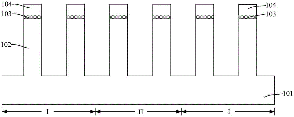
[0034] After research, it is found that the pattern density of each area of the substrate is not exactly the same. According to the pattern density of the substrate surface, the substrate includes a pattern dense area (Dense Area) and a pattern sparse area (ISO Area). The pattern density of the fins located on the substrate surface of the dense area is greater than the pattern density of the fins located on the substrate surface of the sparse area.
[0035] The process steps of forming the fins include: providing an initial substrate including a sparse area and a dense area; forming a patterned mask layer on the surface of the initial substrate, and openings are formed in the patterned mask layer, wherein, The opening size in the mask layer above the sparse area is the first opening size, the opening size in the mask...
PUM
 Abstract
Description
Claims
Application Information


