Semiconductor memory and manufacturing method thereof

A manufacturing method and memory technology, which are applied in the fields of semiconductor devices, semiconductor/solid-state device manufacturing, semiconductor/solid-state device components, etc., can solve the problem of low stacking efficiency of semiconductor memory devices, difficulty in mass production, and multi-layer stacking technology. and other problems, to achieve the effect of large-capacity integration, high integration, and reducing stacking difficulty

Active Publication Date: 2017-05-10
NAT CENT FOR ADVANCED PACKAGING
View PDF6 Cites 10 Cited by
  • Summary
  • Abstract
  • Description
  • Claims
  • Application Information

AI Technical Summary

Problems solved by technology

[0009] In view of this, the embodiments of the present invention provide a semiconductor memory and its manufacturing method to solve the technical problems of low stacking efficiency of semiconductor memory devices, difficulty in realizing multilayer stacking technology, and difficulty in mass production in the prior art

Method used


Image

  • Semiconductor memory and manufacturing method thereof
  • Semiconductor memory and manufacturing method thereof
  • Semiconductor memory and manufacturing method thereof

Examples


Embodiment

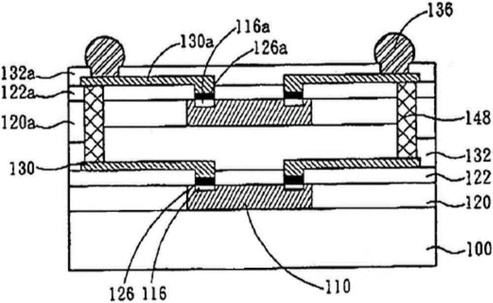
[0048] Figure 4 A schematic structural diagram of a semiconductor memory provided by an embodiment of the present invention. The semiconductor memory provided by the embodiment of the present invention can be used as a cache memory, a main memory, or a stack memory, and the like.

[0049] The semiconductor memory provided in this embodiment includes: two storage chip groups stacked sequentially from bottom to top, the redistribution layers of the two adjacent storage chip groups are electrically connected through the interlayer conductive pillars, and the memory chip located at the bottom The redistribution layer of the chipset is electrically connected to the external connection bump;

[0050] The memory chip group includes two memory chips stacked in sequence, and a composite insulating layer located under the two memory chips, the at least two memory chips are encapsulated in an integrated structure, the rewiring layer is arranged in the composite insulating layer, and th...


PUM


Abstract

The invention discloses a semiconductor memory and a manufacturing method thereof. The semiconductor memory comprises at last two memory chipsets stacked successively from bottom to top, re-wiring layers of two adjacent memory chipsets are electrically connected with inter-layer conductive poles, and a re-wiring layer of the bottommost memory chipset is electrically connected with external connecting projections; and each memory chipset comprises at least two memory chips stacked successively and a composite insulating layer positioned under the memory chips, the memory chips are packed into an integrated structure, the re-wiring layer is arranged in the composite insulating layer, and intra-layer conductive poles of the memory chips are staggered from each other for a preset angle, and are electrically connected with the re-wiring layer. According to the invention, large capacity and high integrated degree of the semiconductor memory are realized, the stacking efficiency of the memory is improved effectively, and the stacking difficulty is reduced.

Description

technical field [0001] Embodiments of the present invention relate to the technical field of semiconductors, and in particular, to a semiconductor memory and a manufacturing method thereof. Background technique [0002] In order to realize the large capacity, high integration and high performance of the memory, a method of stacking memory chips can be used. At present, there are mainly two ways of chip stacking: one is that memory chips are stacked one by one in a dislocation manner, and then each chip is electrically connected together step by step by metal wire bonding. The purpose of using the dislocation structure is to implement metal wire bonding. The other is to vertically stack the memory chips together, and use a through silicon via (Through Silicon Via, TSV) to realize the electrical signal connection between the stacked memory chips. These two methods have obvious defects: chip dislocation stacking and wire bonding, as the number of stacked chips increases, not ...

Claims


Application Information

Patent Timeline
Patent Type & Authority Applications(China)
IPC IPC(8): H01L21/60H01L23/31H01L25/065
CPCH01L24/10H01L25/0657H01L23/3114H01L2224/73267H01L2224/92244H01L2224/97H01L2924/18162H01L21/568H01L2224/04105H01L2224/12105H01L2224/16227H01L2224/19H01L2224/32145
Inventor 陆原陈峰
Owner NAT CENT FOR ADVANCED PACKAGING
Why Eureka
Try Eureka