Separation test method of charge in SiO2 and SiO2/Si interface state

A test method and interface state technology, which are used in semiconductor/solid-state device testing/measurement, circuits, electrical components, etc., can solve the problems of unfavorable promotion and use of separation test methods, and achieve the advantages of popularization and use, low equipment requirements, and simple preparation process. quick effect

Inactive Publication Date: 2017-05-17
INST OF ELECTRONICS ENG CHINA ACAD OF ENG PHYSICS
View PDF4 Cites 8 Cited by
  • Summary
  • Abstract
  • Description
  • Claims
  • Application Information

AI Technical Summary

Problems solved by technology

However, often only large-scale integrated circuit manufacturing companies have ion implanters, and it is difficult for ordinary laboratories to meet such testin...

Method used


Image

  • Separation test method of charge in SiO2 and SiO2/Si interface state
  • Separation test method of charge in SiO2 and SiO2/Si interface state
  • Separation test method of charge in SiO2 and SiO2/Si interface state

Examples


Embodiment 1

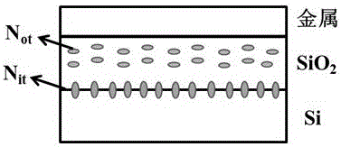
[0028] (1) Using the method of dry oxygen oxidation, grow 150 nm thick SiO on the surface of a p-type silicon wafer with a resistivity of 50 Ω.cm 2 thin film; subsequently, using the method of thermal evaporation on SiO 2 An aluminum thin film is grown on the surface, and then a MIS device is manufactured. The structure diagram of the corresponding MIS device and where N o t and N it distribution, such as figure 1 shown.

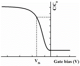
[0029] (2) At normal temperature, carry out C / V test to the MIS device described in step (1), the corresponding C / V curve is as follows figure 1 shown. Obtain the flat band voltage V from the C / V curve fb , and then calculate the total charge density N tot (N tot =N ot + N it ). The corresponding C / V curve is as figure 2 Shown:

[0030] N tot = (W ms -V fb ).C ox (1)

[0031] Among them, N tot is the total charge concentration, N tot =N ot + N it ;W ms is the difference between the metal and semiconductor work functions, and the ...

Embodiment 2

[0038] (1) Using the plasma-enhanced chemical vapor deposition method, a 30 nm thick SiO was grown on the surface of an n-type silicon wafer with a resistivity of 0.1 Ω.cm 2 thin film; subsequently, using the method of magnetron sputtering on SiO 2 A gold film is grown on the surface, and then the MIS device is made;

[0039] (2) At normal temperature, carry out C / V test to the MIS device described in step (1), obtain flat-band voltage V fb , and then calculate the total charge density N tot (N tot =N ot + N it );

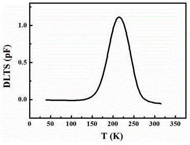
[0040] (3) Further, the deep-level transient spectroscopy (DLTS) test is carried out on the MIS device described in step (1), and the test temperature range is 20-300K. According to the measured deep-level transient spectrum curve, combined with the formula (2), the distribution of the energy level density of the interface state with the energy level is calculated, and the energy level density of the interface state is integrated with the energy level to ob...


PUM

PropertyMeasurementUnit
Resistivityaaaaaaaaaa
Thicknessaaaaaaaaaa

Abstract

The invention provides a separation test method of the charge in SiO2and a SiO2/Si interface state. The separation test method specifically includes the steps of (1) after a SiO2 thin film is grown on the surface of a silicon wafer, growing a metal thin film on the surface of SiO2 to obtain an MIS device; (2) conducting a C/V test of the MIS device to obtain a flat band voltage Vfb, and then calculating the total charge density Ntot; (3) conducting a deep-level transient spectrum test of the MIS device to obtain the distribution of the energy density of the interface state with the energy level, and after integrating, obtaining the total interface state Nit; and (4) subtracting Ntot from Nit to obtain Not, and then achieving the separation test of Not and Nit. The preparation method of the test structure (MIS) used in the invention is simple and quick, has low requirements for equipment, and is conducive to the promotion in science and industry.

Description

technical field [0001] The invention belongs to the technical field of semiconductors, in particular to a SiO 2 Medium charge and SiO 2 / Si interface state separation test method. Background technique [0002] From the birth of the world's first transistor in 1947 to the advent of the world's first integrated circuit in 1958, microelectronics technology has only developed for more than 50 years. Microelectronics technology has changed the entire society and brought about a revolution in information technology. Until now, the characteristic line width of devices in integrated circuits has been decreasing year by year, and continues to develop in accordance with "Moore's Law". In 2014, Intel and Samsung have achieved mass production of 14nm FinFET chips. If Intel can continue to develop according to its established route in the next few years, it will realize 7nm and 5nm process technology in 2017 and 2019 respectively. However, to further reduce the characteristic line wi...

Claims


Application Information

Patent Timeline
IPC IPC(8): H01L21/66
CPCH01L22/14
Inventor 董鹏宋宇李沫侯世尧代刚张健
Owner INST OF ELECTRONICS ENG CHINA ACAD OF ENG PHYSICS
Why Eureka
Try Eureka