Apparatus for realizing semiconductor laser spectrum beam combination by utilizing double gratings

A spectral beam combining and semiconductor technology, which is applied in the field of semiconductor laser spectral beam combining devices, can solve the problems of increasing the focal length of the positive lens, large structure size, and increasing the cavity length of the beam combining system, so as to improve the power and brightness and increase the beam combining Good efficiency and monochromatic effect

Active Publication Date: 2017-05-17
SHANGHAI INST OF OPTICS & FINE MECHANICS CHINESE ACAD OF SCI
View PDF6 Cites 15 Cited by
  • Summary
  • Abstract
  • Description
  • Claims
  • Application Information

AI Technical Summary

Problems solved by technology

In the traditional spectral beam combining technology, there are two ways to compress the spectral broadening: first, reduce the period of the grating, but in order to ensure the diffraction effect of the grating, the minimum period of the grating must be greater than one-half of the light wavelength, which improves the compressed spectrum Limited; second, increase the focal length of the positive lens, but increasing the focal length of the positive lens will increase the cavity length of the beam combining system, multiply the adjustment accuracy and difficulty, and at the same time, the structural size is too large and the stability of the system will be reduced

Method used


Image

  • Apparatus for realizing semiconductor laser spectrum beam combination by utilizing double gratings
  • Apparatus for realizing semiconductor laser spectrum beam combination by utilizing double gratings
  • Apparatus for realizing semiconductor laser spectrum beam combination by utilizing double gratings

Examples


Embodiment

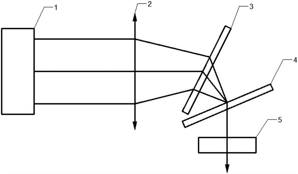
[0031] The specific implementation process of the double grating-based external cavity feedback semiconductor spectral beam combining system of the present invention is as follows:

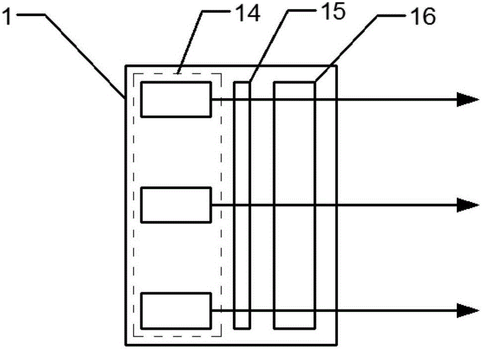
[0032] The center wavelength of semiconductor laser light source 1 is 945nm, including 19 light-emitting units, the fast-axis divergence angle of a single light-emitting point beam is 35°, the slow-axis divergence angle is 7°, and the beam is collimated by a 45° oblique cylindrical lens array and a cylindrical lens After the beam, the divergence angle of the fast axis is compressed to 0.5°, and the divergence angle of the slow axis is compressed to 4°. The front cavity of the laser array is coated with an anti-reflection film, and the reflectivity is less than 0.5%, and the rear cavity is coated with a high-reflection film, and the reflectivity is greater than 99%.

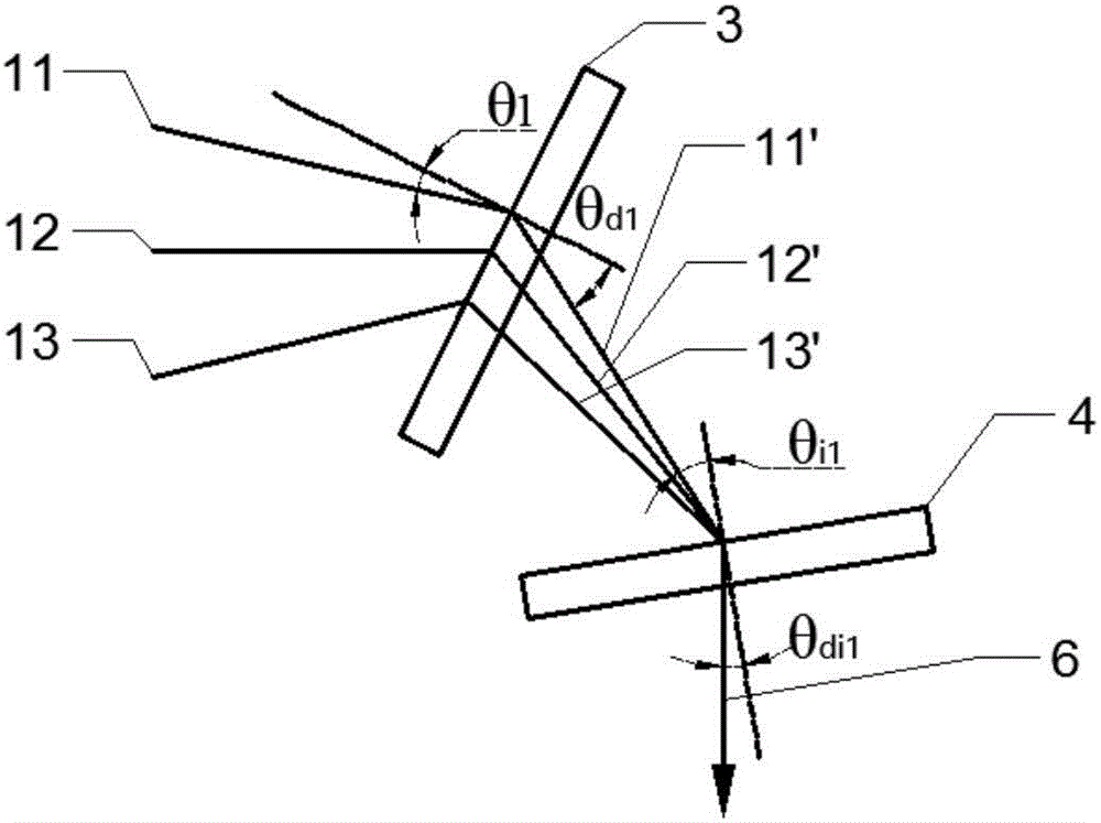
[0033] Let the diffraction order of the first diffraction grating 3 and the second diffraction grating 4 be 1st order, the diffracti...


PUM


Abstract

Disclosed is an apparatus for realizing semiconductor laser spectrum beam combination by utilizing double gratings. The apparatus comprises a semiconductor laser light source, a conversion lens, a first diffraction grating, a second diffraction grating and an output coupling mirror, wherein the semiconductor laser light source emits multiple bunches of parallel light; the light beams are subjected to secondary chromatic dispersion through a diffraction effect of the double gratings; and after the light beams are fed back by the output coupling mirror, the laser of each unit is locked in different wavelengths correspondingly to overlay the respective light beams so as to realize high-power and high-luminance single-beam laser output. By taking the double gratings as a diffraction element, the dispersive power is doubled; when the apparatus is applied to laser spectrum beam combination of the semiconductor laser, the spectrum expansion width can be reduced; by adding more beam combination units to a gain curve of a semiconductor laser gain material, the output power can be improved; and meanwhile, by compressing the length of a resonant cavity, the laser can be compact in structure and the stability can be improved.

Description

technical field [0001] The present invention relates to the technical field of semiconductor lasers, and in particular to a semiconductor laser spectral beam combining method that utilizes double gratings to realize beam combining of multiple semiconductor laser units into high-power and high-brightness laser output through external cavity feedback. device. Background technique [0002] Semiconductor lasers have the advantages of low cost, long life, small size, and high reliability. They have broad application prospects in industrial processing, pumping, medical treatment, and communications. Whether the brightness of semiconductor lasers can be further improved is an important factor restricting the future development of semiconductor lasers. The brightness of the laser beam is determined by the output power and beam quality. The higher the power, the better the beam quality and the higher the brightness. The application fields of semiconductor lasers are also wider. [...

Claims


Application Information

Patent Timeline
Patent Type & Authority Applications(China)
IPC IPC(8): H01S5/06H01S5/40
CPCH01S5/06H01S5/4012
Inventor 周常河周权韦春龙于娜卢炎聪
Owner SHANGHAI INST OF OPTICS & FINE MECHANICS CHINESE ACAD OF SCI
Why Eureka
Try Eureka