Quenching reset circuit for single photon avalanche diode detector

A single-photon avalanche and reset circuit technology, applied in the field of single-photon detection, can solve the problems of easy failure in the quenching process, and achieve the effects of easy handling, steep output pulse and high reliability

Active Publication Date: 2017-05-24
NANJING UNIV OF POSTS & TELECOMM
View PDF4 Cites 13 Cited by
  • Summary
  • Abstract
  • Description
  • Claims
  • Application Information

AI Technical Summary

Problems solved by technology

[0004] Aiming at the problem that the quenching process of the traditional active quenching circuit is prone to failure, the present invention proposes a highly reliable quenching reset circuit,

Method used


Image

  • Quenching reset circuit for single photon avalanche diode detector
  • Quenching reset circuit for single photon avalanche diode detector
  • Quenching reset circuit for single photon avalanche diode detector

Examples


Embodiment Construction

[0017] Below in conjunction with accompanying drawing, the patent of the present invention is described in further detail.

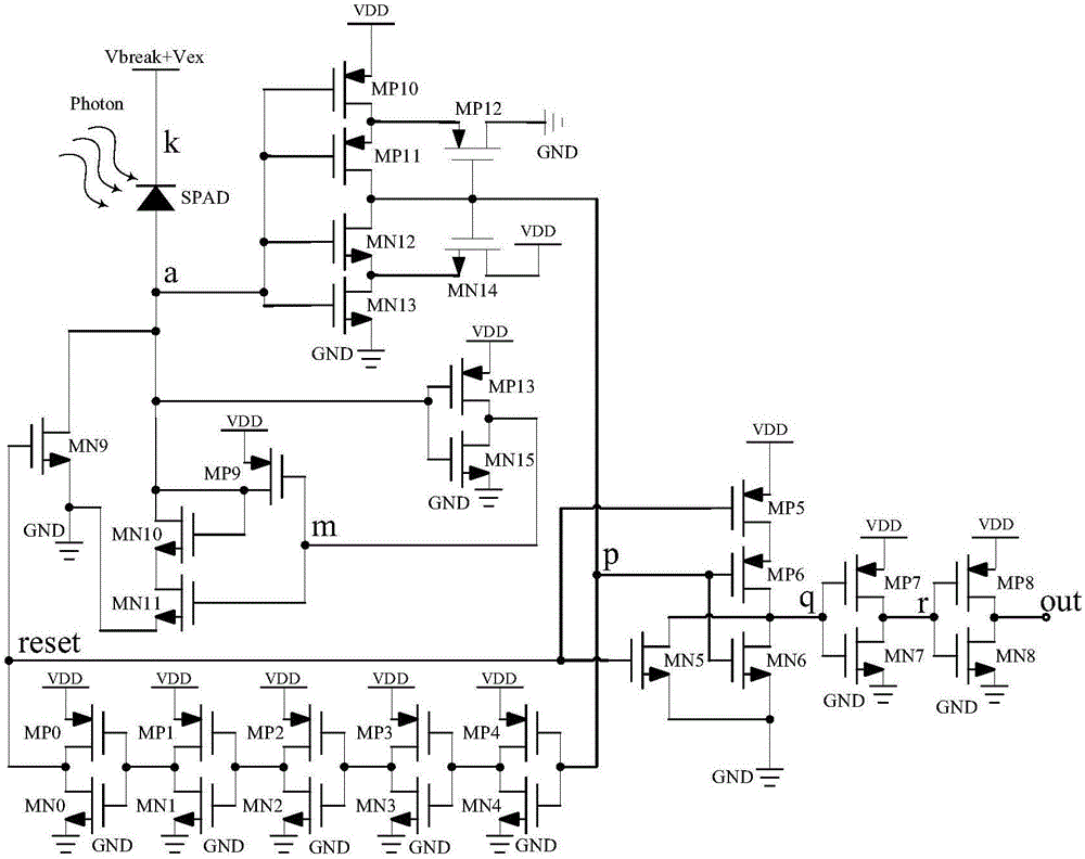
[0018] like figure 1 Shown is the quenching reset circuit diagram of the present invention. The circuit consists of an avalanche diode SPAD, 14 NMOS transistors and 16 PMOS transistors, including: NMOS transistors MN0, MN1, MN2, MN3, MN4, MN5, MN6, MN7, MN8, MN9, MN10, MN11, MN12, MN13, PMOS tubes MP0, MP1, MP2, MP3, MP4, MP5, MP6, MP7, MP8, MP9, MP10, MP11, MP12, MP13, MP14, MP15. where the cathode of the SPAD ( figure 1 K node in the center) is connected to the bias voltage (Vbreak+Vex); the NMOS transistor MN9 is a reset transistor, its gate is connected to the output of the delay circuit (the drain of the PMOS transistor MP0), and the drain is connected to the anode of the diode SPAD ( figure 1 The middle is node a); the drain and gate of the NMOS transistor MN10 are connected together to form a small resistance MOS diode structure, which provides...


PUM


Abstract

The invention discloses a quenching reset circuit for a single photon avalanche diode detector. The reset circuit comprises three parts such as a quenching circuit, a reset circuit and an avalanche signal output portion, and is characterized in that the quenching circuit is composed of five MOS transistors, and the five MOS transistors form a positive feedback circuit for voltage variations of a node a; the reset circuit is composed of 17 MOS transistors; and the avalanche signal output portion is composed of eight MOS transistors. The advantages are that the quenching reset circuit is high in reliability, and a reset operation is ensured to be performed after avalanche current generated by the SPAD (Single Photon Avalanche Diode) detector is sufficiently quenched because of adoption of a Schmitt trigger with high threshold level. In addition, the waveform quality of avalanche pulses generated by the circuit is high, avalanche signals are converted into narrow pulses through a NOR gate, and then the narrow pulses are shaped by a two-stage inverter and act as final output avalanche pulses, so that the output pulses are enabled to be steeper, and processing of a counting circuit is facilitated.

Description

technical field [0001] The invention provides a highly reliable quenching reset circuit and method for a single-photon avalanche photodiode detector, belonging to the technical field of single-photon detection. Background technique [0002] SPAD (Single Photon Avalanche Diode) is a single photon avalanche photodiode. In the field of photodetection, the photomultiplier tube (PMT) in the traditional sense can no longer satisfy the detection under high-speed and low-light conditions. Traditional imaging technology is limited in terms of imaging speed and pixel sensitivity, so solid-state photomultipliers began to appear. tube, the single photon avalanche diode detector. In recent years, using the current standard CMOS process to manufacture high-density, highly integrated SPAD array detectors has become the development trend of this single-photon avalanche diode detector. [0003] A SPAD pixel unit contains two circuits, one is a quenching reset circuit, and the other is a co...

Claims


Application Information

Patent Timeline
Patent Type & Authority Applications(China)
IPC IPC(8): H03K17/22H03K17/78H03K5/01
CPCH03K5/13H03K17/22H03K17/78
Inventor 徐跃李斌罗瑞明李鼎赵庭晨
Owner NANJING UNIV OF POSTS & TELECOMM
Why Eureka
Try Eureka