
Single-trapped-wave ultra-wide-band monopole antenna

A monopole antenna and ultra-wideband technology, which is applied to antennas, resonant antennas, antenna grounding devices, etc., can solve the problems of complex structure processing, increase antenna cross-polarization, increase antenna size, etc., and avoid antenna radiation characteristics. Deterioration, mutual interference suppression, low cost effect

Pending Publication Date: 2017-05-31
中国人民解放军防空兵学院
View PDF11 Cites 10 Cited by
  • Summary
  • Abstract
  • Description
  • Claims
  • Application Information

AI Technical Summary

Problems solved by technology

The disadvantage of this design is that slotting in the radiation part of the antenna will cause the generation of high-order modes, so that the antenna pattern (the graphical representation of the antenna direction function is the pattern of the antenna) is distorted in the high frequency band; at the same time, the surface current is changed The flow path of the antenna also increases the cross-polarization of the antenna, which deteriorates the pattern; (2) carry out band-stop filter design on the feeder, such as the Chinese patent application No. Notch antenna, which utilizes the EBG (Electromagnetic Band-gap) structure symmetrically distributed on both sides of the impedance-matched input microstrip line to achieve band-stop characteristics
The advantage of this method is that the designed band stop structure can be directly embedded into the microstrip line (feeder line), and better band trap performance can be achieved without optimizing other structures; the disadvantage is that the EBG structure additionally adds The size of the antenna is reduced, which is not conducive to miniaturization, and the complex structure puts forward higher requirements for processing

Method used

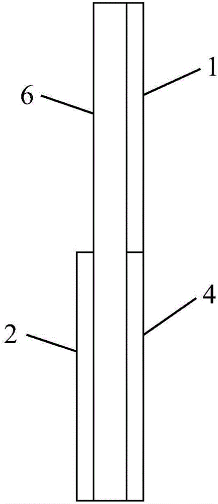
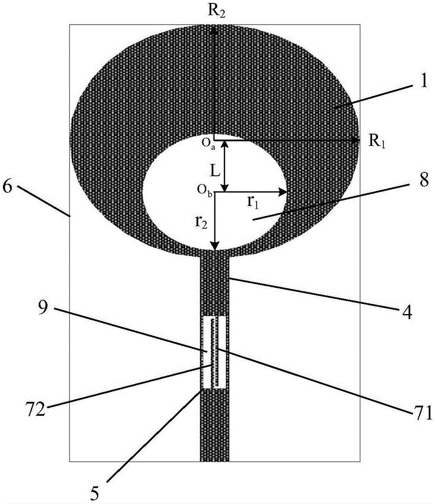
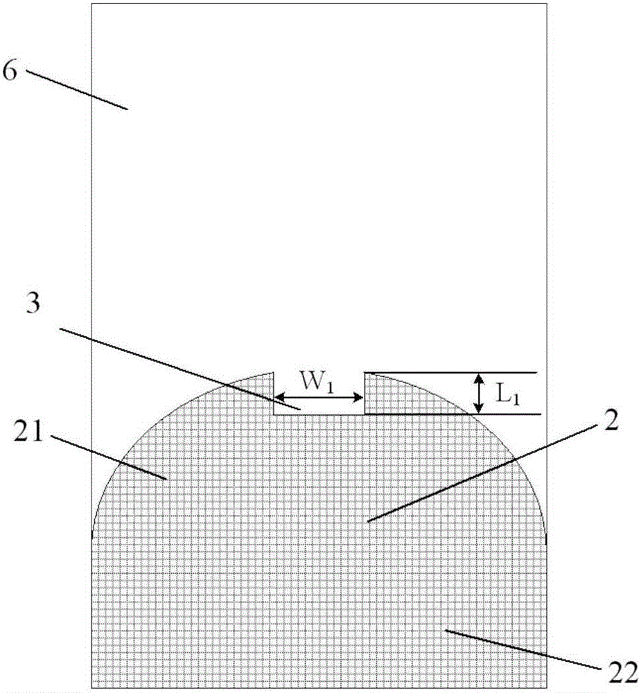

Image

  • Single-trapped-wave ultra-wide-band monopole antenna
  • Single-trapped-wave ultra-wide-band monopole antenna
  • Single-trapped-wave ultra-wide-band monopole antenna

Examples


Embodiment Construction

[0026] In order to facilitate understanding of the present invention, the present invention will be described in more detail below with reference to the accompanying drawings and specific embodiments. Preferred embodiments of the invention are shown in the accompanying drawings. However, the present invention may be embodied in many different forms and is not limited to the embodiments described in this specification. Rather, these embodiments are provided so that a thorough and complete understanding of the present disclosure is provided.

[0027] It should be noted that, unless otherwise defined, all technical and scientific terms used in this specification have the same meaning as commonly understood by those skilled in the technical field of the present invention. The terms used in the description of the present invention are only for the purpose of describing specific embodiments, and are not used to limit the present invention. As used in this specification, the term "...


PUM

PropertyMeasurementUnit
Thicknessaaaaaaaaaa
Lengthaaaaaaaaaa
Widthaaaaaaaaaa

Abstract

The invention discloses a single-trapped-wave ultra-wide-band monopole antenna which comprises a dielectric substrate. A grounding plate is arranged on the lower surface of the dielectric substrate, a radiation patch and a micro-strip feeder line connected with the radiation patch are arranged on the upper surface of the dielectric substrate, and the micro-strip feeder line is etched with a band-elimination resonance unit. The lower portion of the radiation patch is provided with a through hole penetrating through the radiation patch. The micro-strip feeder line of the single-trapped-wave ultra-wide-band monopole antenna is etched with a band-elimination resonance unit, has good trapped-wave properties and can effectively inhibit mutual interference between an ultra-wide band system and a WLAN system, and worsening of radiation characteristics of the antenna due to a mode of etching and grooving on the radiation patch is avoided. The band-elimination resonance unit is simple in structure, compact, small and exquisite and convenient to ingrate, the size of the whole antenna is not additionally increased, and antenna miniaturization can be achieved. The antenna has the advantages of being wide in bandwidth, small in size, low in cost and easy to process and has a good directional diagram in a whole frequency band range.

Description

technical field [0001] The invention belongs to the technical field of antennas, and in particular relates to a single-notch ultra-wideband monopole antenna. Background technique [0002] Ultra-Wide Band (UWB, Ultra-Wide Band) technology is a new type of wireless communication technology. According to the regulations of the Federal Communications Commission (FCC, Federal Communications Commission), the frequency band of UWB communication is 3.1GHz to 10.6GHz. However, this frequency range with a bandwidth of 7.5 GHz includes the current operating frequencies of wireless local area networks (WLAN) 5.2 GHz (5.15 GHz to 5.35 GHz) and 5.8 GHz (5.725 GHz to 5.825 GHz). In order to avoid the interference of signals in these frequency bands, the ultra-wideband antenna needs to be blocked in the frequency band in the range of 5 GHz to 6 GHz, that is, it has a notch (band rejection) characteristic. In addition, the current communication system tends to be miniaturized and highly int...

Claims


Application Information

Patent Timeline
IPC IPC(8): H01Q13/08H01Q9/30H01Q1/36H01Q1/48H01Q1/50
CPCH01Q1/36H01Q1/48H01Q1/50H01Q9/30H01Q13/08
Inventor 李中李天鹏李明明张茜萍高立龙王风华董翔宇孙文波向云强贾博马士友常小龙歹英杰卢亚飞李九林冯少华
Owner 中国人民解放军防空兵学院
Learn More