GaN-based metal-ultrathin oxide-semiconductor composite structure nanolaser and preparation method thereof

A nano-laser, composite structure technology, applied in semiconductor lasers, lasers, laser parts and other directions, can solve the problems of metal-ultra-thin oxide-semiconductor composite structure problems, and achieve small optical mode volume and low lasing threshold. Effect

Inactive Publication Date: 2017-05-31
NANJING UNIV
View PDF4 Cites 8 Cited by
  • Summary
  • Abstract
  • Description
  • Claims
  • Application Information

AI Technical Summary

Problems solved by technology

However, it has always been a difficult problem to realize a large-area, high-quality one-dimensional InGaN / GaN nanowire array and prepare a metal-ultra-thin oxide-semiconductor (MUTOS) composite structure. At present, there are no relevant invention patents in China to query and refer to.

Method used


Image

  • GaN-based metal-ultrathin oxide-semiconductor composite structure nanolaser and preparation method thereof
  • GaN-based metal-ultrathin oxide-semiconductor composite structure nanolaser and preparation method thereof
  • GaN-based metal-ultrathin oxide-semiconductor composite structure nanolaser and preparation method thereof

Examples


Embodiment 1

[0050] The preparation method of the GaN-based metal-ultra-thin oxide-semiconductor composite structure nano-laser, the steps include:

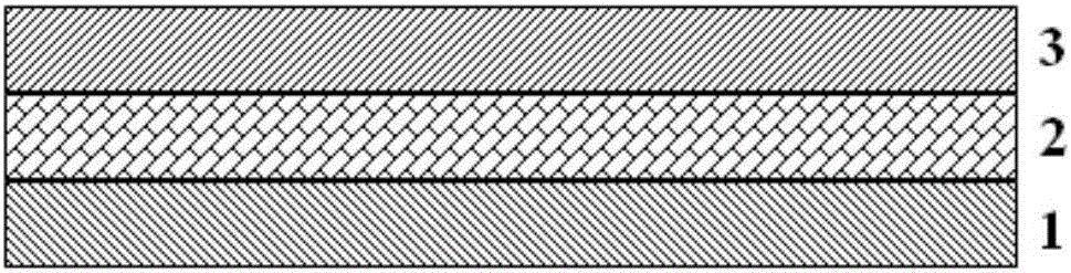
[0051] (1) A layer of SiO is grown on the InGaN / GaN quantum well epitaxial wafer 2 For the insulating layer, spin-coat PMMA glue and UV-curable glue on the surface of the insulating layer in sequence. The thickness of PMMA glue is 200nm, and the thickness of UV-curable glue is 30nm. The structure of the InGaN / GaN quantum well epitaxial wafer includes: a sapphire substrate layer , an n-type GaN layer 1 grown on the substrate layer, an In grown on the n-type GaN layer x Ga 1-x N / GaN quantum well active layer 2, grown on In x Ga 1-x The p-type AlGaN barrier layer and p-type GaN layer 3 on the N / GaN quantum well active layer, where x=0.23, the quantum well active layer emits light at a wavelength of 490nm, the number of periods of the quantum well is 10, and the p-type AlGaN barrier layer and the total thickness of the p-type GaN layer is 300...

Embodiment 2

[0062] The preparation method of the GaN-based metal-ultra-thin oxide-semiconductor composite structure nano-laser, the steps include:

[0063] (1) A layer of SiC insulating layer is grown on the InGaN / GaN quantum well epitaxial wafer, and PMMA glue and UV curing glue are spin-coated on the surface of the insulating layer in turn. The thickness of PMMA glue is 600nm, and the thickness of UV curing glue is 300nm. InGaN / GaN quantum In the well epitaxial wafer, x=0.35, the quantum well active layer emits light at a wavelength of 530nm, the number of periods of the quantum well is 15, and the total thickness of the p-type AlGaN barrier layer and the p-type GaN layer is 500nm;

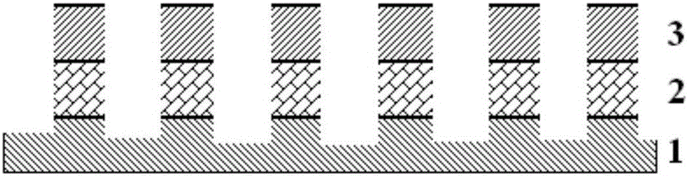
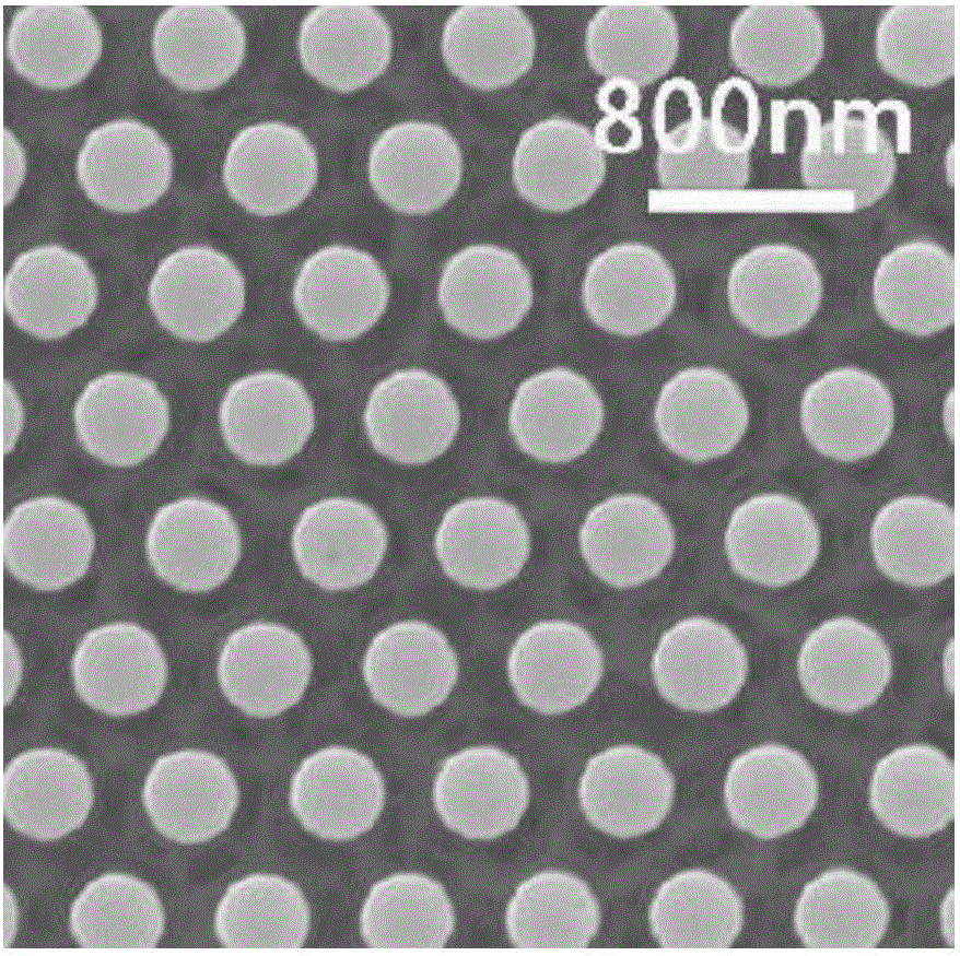
[0064] (2) Using UV soft nanoimprinting technology, a soft template is used to form a large-area ordered nano-elliptical column array on the UV-cured adhesive layer. The long-axis diameter of the nano-elliptical column is 240nm, the short-axis diameter is 160nm, and the period is 550nm. , arranged in hexago...

Embodiment 3

[0074] The preparation method of the GaN-based metal-ultra-thin oxide-semiconductor composite structure nano-laser, the steps include:

[0075] (1) A layer of SiC insulating layer is grown on the InGaN / GaN quantum well epitaxial wafer, PMMA glue and UV curing glue are spin-coated on the surface of the insulating layer in turn, the thickness of PMMA glue is 400nm, and the thickness of UV curing glue is 150nm. InGaN / GaN quantum In the well epitaxial wafer, x=0.20, the light emission wavelength of the active layer of the quantum well is 480nm, the period number of the quantum well is 12, and the total thickness of the p-type AlGaN barrier layer and the p-type GaN layer is 400nm;

[0076](2) Using UV soft nanoimprinting technology, a soft template is used to form a large-area ordered nano-elliptical column array on the UV-cured adhesive layer. The long-axis diameter of the nano-elliptical column is 240nm, the short-axis diameter is 160nm, and the period is 550nm. , arranged in hex...


PUM

PropertyMeasurementUnit
emission peakaaaaaaaaaa
thicknessaaaaaaaaaa
diameteraaaaaaaaaa

Abstract

The invention discloses a GaN-based metal-ultrathin oxide-semiconductor composite structure nanolaser, which comprises a substrate and an InGaN / Ga quantum well nano-column, wherein the structure of the substrate sequentially comprises a SiO2-Si substrate, a metal layer and an ultrathin oxide layer; the InGaN / Ga quantum well nano-column is put on the surface of the ultrathin oxide layer and structure of the InGaN / Ga quantum well nano-column sequentially comprises a sapphire substrate layer, an n-type GaN layer, an In<x>Ga<x-1>N / GaN quantum well active layer and a p-type GaN layer. The invention further discloses a preparation method of the GaN-based metal-ultrathin oxide-semiconductor composite structure nanolaser. The nanolaser has the advantages that (1) the nanolaser has very small optical mode volume and can break through a diffraction limit of light, and the submicron-sized laser can be achieved; (2) the laser has an extremely low lasing threshold and an MUTOS laser light structure can lase under an optical pump of 0.15kW / cm<2>; and (3) the mode of laser light can be regulated and controlled and single-mode and multi-mode laser light transmission is achieved. The laser structure has potential application value in the aspects of ultra-high resolution intelligent displaying, complicated biological imaging, and photoelectric interconnection of a silicon-based integration circuit and a photoelectronic device.

Description

technical field [0001] The patent of the invention relates to a GaN-based metal-ultra-thin oxide-semiconductor composite structure nano-laser and its preparation method, belonging to the application field of micro-nano optoelectronics and laser devices. Background technique [0002] Group III nitride semiconductors have continuously adjustable wide energy gaps, which have considerable advantages in blue-green and ultraviolet optoelectronic devices. In order to improve the efficiency of light-emitting devices and expand the functions of devices, researchers have used a large number of low-dimensional quantum structures, including quantum wells, quantum wires (nanowires), nanodots and other structures, and at the same time enable devices to be used in mechanical, biochemical, electromagnetic and optoelectronic and other aspects to demonstrate excellent performance. The one-dimensional nanowire (column) quantum structure forms an optical microcavity because of its good optical...

Claims


Application Information

Patent Timeline
Patent Type & Authority Applications(China)
IPC IPC(8): H01S5/30H01S5/343
CPCH01S5/34333H01S5/3013
Inventor 刘斌陶涛智婷张荣谢自力陈鹏陈敦军韩平施毅郑有炓
Owner NANJING UNIV
Why Eureka
Try Eureka