Method for improving LED (light emitting diode) photoelectric characteristics by utilizing V type defects
A technology for photoelectric characteristics and defects, applied in circuits, electrical components, semiconductor devices, etc., can solve problems such as deterioration of photoelectric performance of LED devices, achieve the effect of improving photoelectric characteristics, increasing luminous efficiency, and the method is simple and feasible
- Summary
- Abstract
- Description
- Claims
- Application Information
AI Technical Summary
Problems solved by technology
Method used
Image

Examples
Embodiment 1
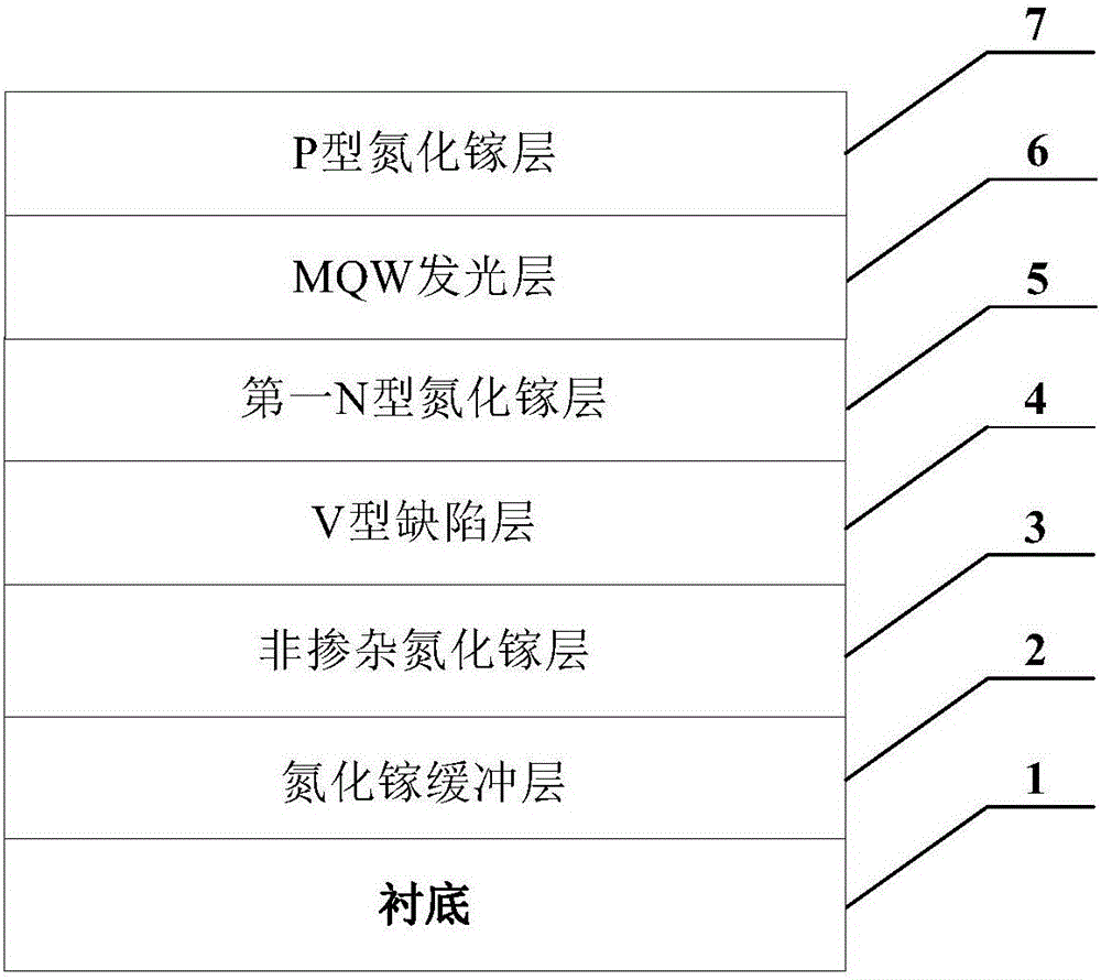
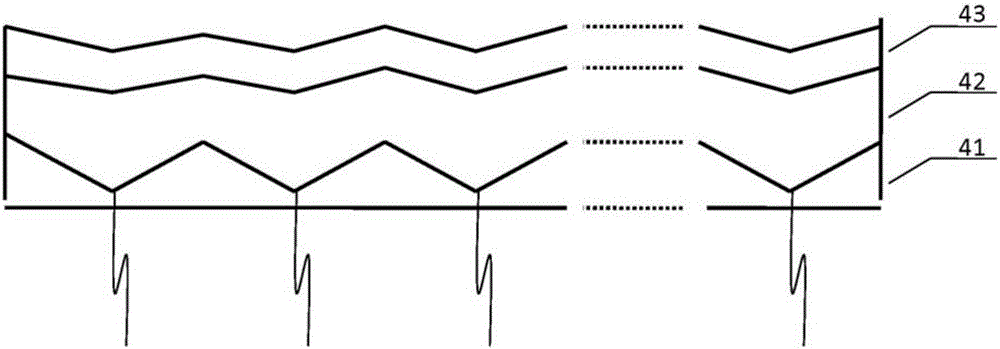
[0043] This embodiment provides a method for improving the photoelectric characteristics of LEDs by using V-shaped defects, please refer to figure 2 and image 3 , including:
[0044] 1. Growing a gallium nitride buffer layer 2 and a non-doped gallium nitride layer 3 sequentially on a substrate 1, wherein the substrate 1 is a sapphire substrate.
[0045] 2. A shallow well layer 41 is grown on the surface of the non-doped gallium nitride layer 3, and the material of the shallow well layer 41 is In 0.2 Ga 0.8 N, the thickness is The growth conditions are: the pressure is about 200 torr, and the temperature is about 820°C.
[0046] 3. A second N-type gallium nitride layer 42 is grown on the surface of the shallow well layer 41 with a thickness of The doping concentration of Si is 5×10 18 / cm 3 , the growth conditions are: the pressure is about 200 torr, and the temperature is about 820°C.
[0047] 4. Growing a layer of N-type GaN aluminum layer 43 on the surface of the...
Embodiment 2
[0055] This embodiment provides a method for improving the photoelectric characteristics of LEDs by using V-shaped defects, please refer to figure 2 and Figure 4 , including:
[0056] 1. Growing a gallium nitride buffer layer 2 and a non-doped gallium nitride layer 3 sequentially on a substrate 1, wherein the substrate 1 is a sapphire substrate.
[0057] 2. A shallow well layer 41 is grown on the surface of the non-doped gallium nitride layer 3, and the material of the shallow well layer 41 is In 0.2 Ga 0.8 N, the thickness is The pressure is about 200 torr and the temperature is about 820°C.
[0058] 3. A second N-type gallium nitride layer 42 is grown on the surface of the shallow well layer 41 with a thickness of The doping of Si is 5×10 18 / cm 3 , the pressure is about 500torr, and the temperature is about 820°C.
[0059] 4. Growing a layer of N-type GaN aluminum layer 43 on the surface of the second N-type GaN layer 42 with a thickness of The doping of Si is...
Embodiment 3
[0067] This embodiment provides a method for improving the photoelectric characteristics of LEDs by using V-shaped defects, please refer to figure 2 and Figure 5 , including:
[0068] 1. Growing a gallium nitride buffer layer 2 and a non-doped gallium nitride layer 3 sequentially on a substrate 1, wherein the substrate 1 is a sapphire substrate.
[0069] 2. A shallow well layer 41 is grown on the surface of the non-doped gallium nitride layer 3, and the material of the shallow well layer 41 is In 0.2 Ga 0.8 N, the thickness is The pressure is about 200 torr and the temperature is about 820°C.
[0070] 3. A second N-type gallium nitride layer 42 is grown on the surface of the shallow well layer 41 with a thickness of The doping concentration of Si is 5×10 18 / cm 3 , and, during the growth process of the second N-type gallium nitride layer 42 , the temperature is maintained at about 820° C., and the pressure is gradually increased from 200 torr to 500 torr.
[0071] ...
PUM
| Property | Measurement | Unit |
|---|---|---|
| Doping concentration | aaaaa | aaaaa |
Abstract
Description
Claims
Application Information
 - R&D
- Intellectual Property
- Life Sciences
- Materials
- Tech Scout
- Unparalleled Data Quality
- Higher Quality Content
- 60% Fewer Hallucinations
Browse by: Latest US Patents, China's latest patents, Technical Efficacy Thesaurus, Application Domain, Technology Topic, Popular Technical Reports.
© 2025 PatSnap. All rights reserved.Legal|Privacy policy|Modern Slavery Act Transparency Statement|Sitemap|About US| Contact US: help@patsnap.com