
Method for strengthening Cr-doped ZnO thin film ferromagnetism through Ar particle irradiation

A ferromagnetic and irradiation technology, applied in the application of conductive/insulating/magnetic materials on magnetic films, magnetic objects, magnetic materials, etc., can solve the problems of low spin electron injection efficiency and low saturation magnetization, and achieve The method is stable and effective, and the effect of ferromagnetic enhancement

Inactive Publication Date: 2017-07-04
SHANGHAI INST OF CERAMIC CHEM & TECH CHINESE ACAD OF SCI
View PDF2 Cites 6 Cited by
  • Summary
  • Abstract
  • Description
  • Claims
  • Application Information

AI Technical Summary

Problems solved by technology

[0009] The present invention mainly aims at the problem that the current saturation magnetization of Cr-doped ZnO film is not high, and the injection efficiency of spin electrons is low. The purpose of the present invention is to provide a method for improving such problems

Method used


Image

  • Method for strengthening Cr-doped ZnO thin film ferromagnetism through Ar particle irradiation
  • Method for strengthening Cr-doped ZnO thin film ferromagnetism through Ar particle irradiation
  • Method for strengthening Cr-doped ZnO thin film ferromagnetism through Ar particle irradiation

Examples


preparation example Construction

[0038] The preparation method of the Cr-doped ZnO thin film comprises: clean and dry substrate, Zn 1-x Cr x The O target is placed in the chamber. Vacuum the chamber background to ≤5.0×10 -4 Pa, feed high-purity Ar at a flow rate of 20-30 sccm, adjust the pressure of the cavity at 1.0-1.5 Pa, and then heat the substrate to 300-350°C. Finally, turn on the radio frequency power supply, and sputter for 1.5-2 hours at a power of 100-150W. In one example, the deposition step may include: (1) Si substrate and Zn 1-x Cr x O (0 -4 Pa, and then heat the Si substrate to 300 °C, and then vacuum the chamber background to ≤5.0×10 -4 Pa. (3) By introducing high-purity Ar gas at a flow rate of 20 sccm, adjust the pressure of the cavity to 1.0 Pa, turn on the radio frequency power supply, and deposit at a power of 150 W for 2 hours. (4) After the preparation is completed, the temperature is naturally lowered to room temperature, and the prepared film sample is taken out.

[0039] Zn w...

Embodiment 1

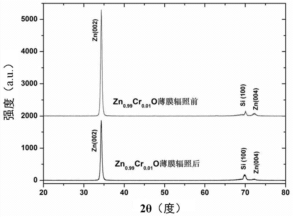
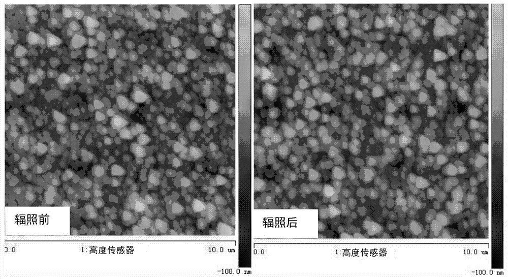
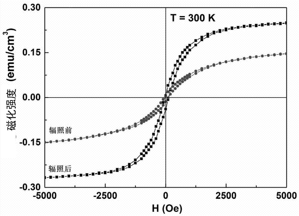
[0050] (1) Put the Si substrate in acetone for ultrasonic cleaning for 15 minutes, and then rinse it with deionized water for 10 minutes; 2) put the Si substrate in alcohol for ultrasonic cleaning for 15 minutes, and then rinse it with deionized water for 10 minutes; (3) High purity N for substrate 2 Dry; (4) Si substrate, Zn 0.99 Cr 0.01 O The target is placed in the chamber; (5) The background vacuum of the chamber is evacuated to ≤5.0×10 -4 Pa, feed high-purity Ar at a flow rate of 20sccm, and maintain the chamber pressure at 1.0Pa, then heat the sapphire substrate to 300°C; (6) finally turn on the radio frequency power supply, and sputter for 2.0h at a power of 150W , get Zn 0.99 Cr 0.01 O film with a thickness of 450nm; (7) at room temperature, with an energy of 2.8MeV and a dose of 7×10 14 cm -2 The Ar particle flow is used to modify the film by irradiation; (8) The magnetic test results show that the room temperature saturation magnetization of the film after irra...

Embodiment 2

[0052] (1) Put the Si substrate in acetone for ultrasonic cleaning for 15 minutes, and then rinse it with deionized water for 10 minutes; 2) put the Si substrate in alcohol for ultrasonic cleaning for 15 minutes, and then rinse it with deionized water for 10 minutes; (3) High purity N for substrate 2 Dry; (4) Si substrate, Zn 0.95 Cr 0.05 O The target is placed in the chamber; (5) The background vacuum of the chamber is evacuated to ≤5.0×10⁻⁴ Pa, feed high-purity Ar at a flow rate of 20sccm, and maintain the chamber pressure at 1.0Pa, then heat the sapphire substrate to 300°C; (6) finally turn on the radio frequency power supply, and sputter for 2.0h at a power of 150W , get Zn 0.95 Cr 0.05 O thin film with a thickness of 450nm; (7) at room temperature with an energy of 2.8MeV and a dose of 5×10 16 cm -2 The Ar particle flow is used to modify the film by irradiation; (8) The magnetic test results show that the room temperature saturation magnetization of the film after ir...


PUM

PropertyMeasurementUnit
thicknessaaaaaaaaaa

Abstract

The invention relates to a method for strengthening Cr-doped ZnO thin film ferromagnetism through Ar particle irradiation. A Cr-doped ZnO thin film is subjected to irradiation by a certain dosage of Ar particles; and the chemical formula of the Cr-doped ZnO thin film is Zn<1-x>Cr<x>O, wherein x is greater than 0 and less than or equal to 0.05. The method is stable and effective, and the ferromagnetism of a ZnO-based diluted magnetic semiconductor thin film can be obviously strengthened without damaging the material, so that development of a spinning electronic device based on a diluted magnetic semiconductor material can be facilitated.

Description

technical field [0001] The invention relates to a method for enhancing the ferromagnetism of a Cr-doped ZnO thin film by Ar particle irradiation, and belongs to the field of new functional semiconductor materials. Background technique [0002] Diluted magnetic semiconductor generally refers to a new type of functional semiconductor material formed by introducing metal elements with 3d or 4f electrons to partially replace nonmagnetic ions in nonmagnetic semiconductor materials. Traditional semiconductor devices only use the charge properties of electrons, and magnetic memory device materials only use the spin properties of electrons. Currently, spintronic devices that have attracted much attention can use both the charge and spin properties of electrons. Spintronic devices have the advantages of non-volatility, fast speed, small size, and low energy consumption, and are considered to be the most promising new electronic devices in the future, such as spin field effect transis...

Claims


Application Information

Patent Timeline
Patent Type & Authority Applications(China)
IPC IPC(8): H01F1/40H01F41/32C23C14/34C23C14/08
CPCH01F1/402C23C14/08C23C14/34H01F41/325
Inventor 刘学超陈卫宾卓世异施尔畏
Owner SHANGHAI INST OF CERAMIC CHEM & TECH CHINESE ACAD OF SCI
Learn More