Split type crucible for crystal growth of silicon carbide

A technology of crystal growth and silicon carbide, applied in the direction of crystal growth, single crystal growth, single crystal growth, etc., can solve the problems of temperature gradient change, temperature gradient instability, seed crystal sublimation damage, etc.

Inactive Publication Date: 2017-07-07
SHANGHAI INST OF CERAMIC CHEM & TECH CHINESE ACAD OF SCI
View PDF7 Cites 14 Cited by
  • Summary
  • Abstract
  • Description
  • Claims
  • Application Information

AI Technical Summary

Problems solved by technology

[0005] However, a large number of experiments have found that in the early stage of crystal growth, due to the inevitable process of temperature rise and depressurization process control, there are certain problems of unstable temperature gradient and insufficient transport of gas phase components inside the crucible, which leads to sublimation damage of the seed crystal, and in the crystal growth introduces a large number of defects in
In addition, as the crystal growth process progresses, the crystal gradually thickens, and the distance between the crystal surface and the raw material surface shrinks, which also leads to changes in the temperature gradient inside the crucible, often causing polymorphic derivatives and other crystal defects.

Method used


Image

  • Split type crucible for crystal growth of silicon carbide
  • Split type crucible for crystal growth of silicon carbide
  • Split type crucible for crystal growth of silicon carbide

Examples


Embodiment 1

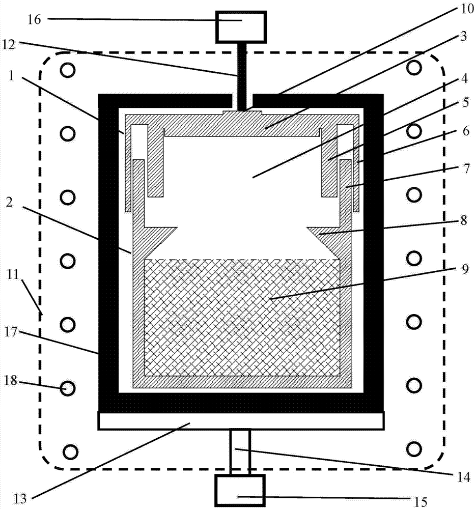
[0081] Using high-purity graphite material (purity>99.9%) to prepare such as figure 1 In the SiC crystal growth crucible with the structure shown, the gap between the adjacent surfaces of the growth chamber 5 , the outer cylinder 6 and the guide cylinder 7 is 0.5 mm. The specific structure is as described above. The crucible with this structure can control the rise and fall of the growth chamber 1 during the crystal growth process, control the position of the seed crystal in the crystal seeding stage in the early growth stage, adjust the distance between the crystal growth surface and the raw material during the growth process, and grow high-quality SiC crystals.

Embodiment 2

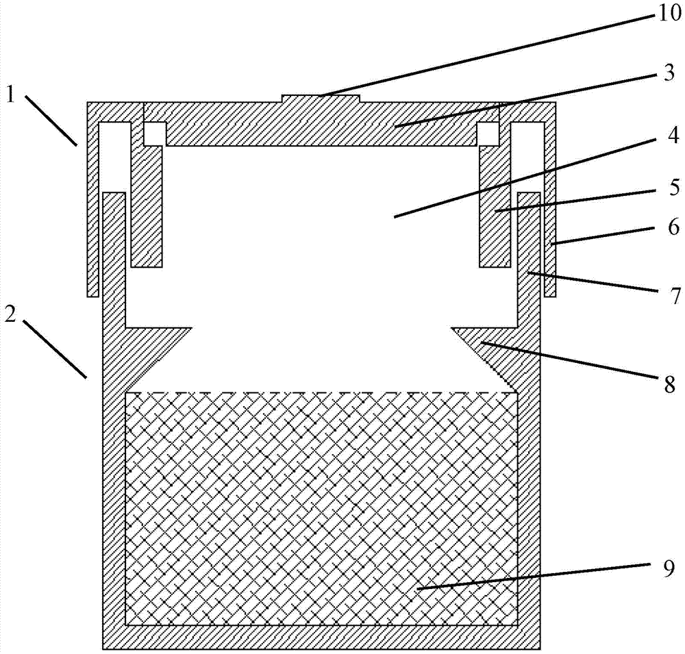
[0083] Using high-purity graphite material (purity>99.9%) to prepare such as figure 2 The crucible for SiC crystal growth with the structure shown, wherein the growth chamber 1 includes a seed crystal holder 3, a growth chamber 4, a growth chamber cylinder 5, and a growth chamber cylinder 6; Sheng raw materials9.

[0084] In this embodiment, there is a cavity structure between the top of the tube 5 in the growth chamber and the seed crystal holder 3, which is a space for the crystallization of redundant gas phase components; at the same time, to realize this design, the growth chamber 1 is composed of a plurality of different components.

[0085] When the growth cavity 1 and the raw material cavity 2 are combined, the growth cavity 1 is set on the guide cylinder 7, and the gap between the two adjacent surfaces is 0.1mm, and the two can slide and rotate relatively freely.

[0086] The top of the growth chamber 1 is provided with a connecting portion connected with correspondi...

Embodiment 3

[0089] Using tantalum (elemental metal) (purity>99.9%) to prepare as figure 1 For the crucible for SiC crystal growth with the structure shown, please refer to the previous description for the specific structure. The gap between the adjacent surfaces of the growth chamber cylinder 5, the outer cylinder 6 and the guide cylinder 7 is 1 mm. The use of tantalum crucibles can prevent the C element in the graphite crucible from becoming part of the C source for SiC crystal growth, which is more conducive to the control of gas phase components, and can also control the rise and fall of the growth chamber 1 during the crystal growth process, and crystal seeding in the early growth stage The stage controls the position of the seed crystal, adjusts the distance between the crystal growth surface and the raw material during the growth process, and finally grows a high-quality SiC crystal.


PUM


Abstract

The invention provides a split type crucible for crystal growth of silicon carbide. The crucible comprises the following components: a raw material chamber for containing raw materials for crystal growth of SiC; a growth chamber which is nested on the upper part of the raw material chamber in relative movement mode in order to form a crystallization area of crystal, wherein the growth chamber comprises a growth chamber, and a seed crystal holder which is arranged on a upper wall of the growth chamber; and a double layer structure which is formed by sidewalls of the growth chamber and comprises an inner cylinder and an outer cylinder. The crucible can be used for adjusting distance between the crystal surface and the raw material surface in a process of growth, and the stability of a temperature field is kept.

Description

technical field [0001] The invention belongs to the field of crystal growth, and relates to a crucible structure for growing SiC crystals by using a physical vapor transport method, in particular to a split-type silicon carbide crystal growth crucible. Background technique [0002] SiC crystal has a series of advantages such as large band gap, strong critical breakdown field, high saturation drift speed, low thermal expansion coefficient, and strong radiation resistance. It is a new generation of semiconductor materials that have attracted much attention. Substrate and other applications have broad application prospects. Especially in the past ten years, both SiC crystal materials and related device application research have made great progress, and SiC crystal devices have gradually entered power electronics, new energy vehicles, LED lighting and other industries. [0003] SiC crystal growth generally adopts the physical vapor transport method (physical vapor transport, PV...

Claims


Application Information

Patent Timeline
Patent Type & Authority Applications(China)
IPC IPC(8): C30B23/00C30B29/36
CPCC30B23/00C30B29/36
Inventor 孔海宽忻隽陈建军郑燕青施尔畏
Owner SHANGHAI INST OF CERAMIC CHEM & TECH CHINESE ACAD OF SCI
Why Eureka
Try Eureka