IGBT device and preparation method thereof

A device and semiconductor technology, applied in the field of power semiconductor devices, can solve problems such as breakdown voltage reduction, cell damage, and easy failure, so as to achieve stable breakdown characteristics and improve avalanche tolerance

Active Publication Date: 2017-08-01
安建科技(深圳)有限公司
View PDF4 Cites 9 Cited by
  • Summary
  • Abstract
  • Description
  • Claims
  • Application Information

AI Technical Summary

Problems solved by technology

Due to the negative resistance breakdown characteristics of the IGBT device 200, as the avalanche current increases, the breakdown voltage of these cells will be further reduced, causing the breakdown current to be locally concentrated in these cells, which can easily cause damage to the cells
Therefore, this causes the avalanche withstand capacity of the IGBT device 200 to be low, making the device prone to failure in practical applications

Method used


Image

  • IGBT device and preparation method thereof
  • IGBT device and preparation method thereof
  • IGBT device and preparation method thereof

Examples


Embodiment 1

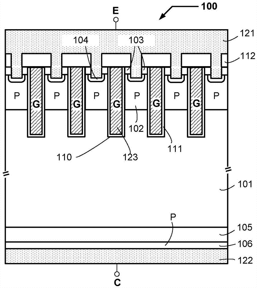
[0027] Figure 4 Shown in is a schematic diagram of the cross-sectional structure of the IGBT device 300 according to the first embodiment of the present invention. The structure of the device 300 includes: a collector (122) (C pole) is located at the bottom of the device, and a p-type collector layer (106) (ie, the first semiconductor layer of the first conductivity type) is located between the collector (122) on; an n-type buffer layer (105) (that is, the second semiconductor layer of the second conductivity type) is located on the p-type collector layer (106); an n - type drift region (101) (that is, the third semiconductor region of the second conductivity type) is located on the n-type buffer layer (105); one or more parts are partially covered by the n-type - The trenches with different structural characteristics closed by the upper surface of the type drift region (101): the trenches include gate trenches (110) with a deep trench depth (that is, the first type of trenc...

Embodiment 2

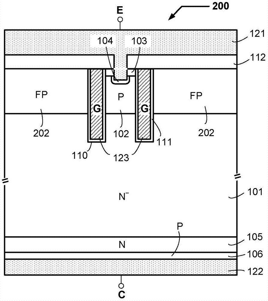
[0034] Figure 17 Shown in is a schematic diagram of the cross-sectional structure of the IGBT device 400 according to the second embodiment of the present invention. It should be pointed out that in Figure 17 structure shown, with the above Figure 4 The same or equivalent structures shown in are given the same symbols, and descriptions of these symbols may not be repeated here. Similar to the device 300 described in the first embodiment, a feature of the device 400 is that it has a series of trenches with different structural features, including a deeper gate trench (110) and a shallower dummy trench (210), to Improve the avalanche tolerance and reliability of the device. However, device 400 also has another characteristic, that is, the lateral spacing between adjacent gate grooves (110) (not in Figure 17 shown in ), and the lateral spacing between the gate groove (110) and the adjacent dummy groove (210) ( Figure 17 marked as "m") are greater than the lateral spacin...

Embodiment 3

[0036] Figure 18 Shown in is a schematic diagram of the cross-sectional structure of the IGBT device 500 according to the third embodiment of the present invention. It should be pointed out that in Figure 18 structure shown, with the above Figure 4 to Figure 17 The same or equivalent structures shown in are given the same symbols, and descriptions of these symbols may not be repeated here. Similar to the device 300 described in the first embodiment, a feature of the device 500 is that it has a series of trenches with different structural features, including a deeper gate trench (110) and a shallower dummy trench (210), to Improve the avalanche tolerance and reliability of the device. However, the device 500 also has another characteristic, that is, no electrically floating p-region ( 202 ) is set between adjacent dummy slots ( 210 ). Since the electrically floating p-region ( 202 ) cannot effectively support the voltage when the device is turned off, removing this regio...


PUM


Abstract

The invention discloses an IGBT device and a preparation method thereof, relates to a power semiconductor device, and provides a device structure design scheme capable of improving avalanche tolerance on the basis of not lowering other performance indexes (such as forward conduction voltage drop V<on>, switching speed, load short-circuit capacity and the like) of the IGBT. The invention provides a novel IGBT device structure and a preparation method thereof. Beneficial effects are achieved as follows: compared with the IGBT device in the prior art, the IGBT device disclosed by the invention can realize more stable breakdown characteristic, so that the avalanche tolerance of the device can be greatly improved, thereby enabling the device to the safer and more reliable in an actual high-speed high-power application.

Description

technical field [0001] The invention relates to a power semiconductor device, in particular to an IGBT device and a preparation method thereof. Background technique [0002] As a key power semiconductor device, insulated gate bipolar transistor (hereinafter referred to as "IGBT") is widely used in various medium and high voltage power switching applications, such as motor drive and power conversion, etc., in these and other In related applications, a power load driven by an IGBT is often an inductive load. During the high-speed switching process, the overshoot voltage induced by the inductance may cause the IGBT device to enter the avalanche breakdown state, which will lead to device damage and failure. Therefore, the IGBT device is required to have a certain tolerance to the avalanche breakdown state. This capability is quantified as the avalanche endurance of the IGBT. For the latest generation of IGBT devices, because they work at higher current densities and faster swi...

Claims


Application Information

Patent Timeline
Patent Type & Authority Applications(China)
IPC IPC(8): H01L29/06H01L29/423H01L29/739H01L21/331H01L21/28
Inventor 单建安冯浩
Owner 安建科技(深圳)有限公司
Why Eureka
Try Eureka