MoS2 photoelectric detector based on Fe-doped GaN substrate and manufacturing method

A technology of photodetectors and molybdenum disulfide, applied in circuits, electrical components, semiconductor devices, etc., can solve the problems of reducing the detection efficiency of the detector and reducing the detection efficiency

Inactive Publication Date: 2017-08-08
SHENZHEN UNIV
View PDF4 Cites 4 Cited by
  • Summary
  • Abstract
  • Description
  • Claims
  • Application Information

AI Technical Summary

Problems solved by technology

For p-n junction detectors, the carriers generated when the incident light is absorbed need to diffuse into the depletion region and then be separated by the electric field in the depletion region. In this process, the existence of non-radiative recombination centers such as interface defects cannot A large number of non-radiative recombination of carriers will be avoided, which will reduce the detection efficiency of the detector
For metal-semiconductor Schottky detectors, the metal forming the Schottky contact on the upper surface will inevitably reflect the incident light, thereby reducing the detection efficiency.

Method used


Image

  • MoS2 photoelectric detector based on Fe-doped GaN substrate and manufacturing method
  • MoS2 photoelectric detector based on Fe-doped GaN substrate and manufacturing method
  • MoS2 photoelectric detector based on Fe-doped GaN substrate and manufacturing method

Examples


Embodiment Construction

[0019] The present invention will be described in detail below in conjunction with the accompanying drawings and specific embodiments.

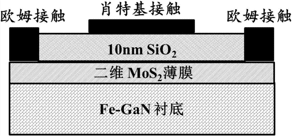
[0020] This embodiment provides a method for preparing a molybdenum disulfide photodetector based on an Fe-doped GaN substrate. The preparation method includes, first, cleaning the Fe-doped GaN substrate. The specific clear process of the Fe-doped GaN substrate is as follows:

[0021] First use acetone ultrasonic cleaning, the ultrasonic frequency of cleaning is 45~50KHz, then, use ethanol ultrasonic cleaning, the ultrasonic frequency of cleaning is 50~55KHz, then use deionized water, rinse in a beaker, and then in sulfuric acid: nitric acid = Boil in a 1:1 volume ratio mixture at 80°C for several minutes, rinse with deionized water, in which the concentration of sulfuric acid is 98%, and the concentration of nitric acid is 98%; then in hydrochloric acid: hydrogen peroxide: water = 3:1:1 volume Shake gently for several minutes in the mixed so...


PUM


Abstract

The invention discloses a MoS2 photoelectric detector based on Fe-doped GaN substrate and a manufacturing method. The method includes the following steps: a MoS2 film layer growing on the surface of a Fe-doped GaN substrate; and a SiO2 layer growing on the surface of the MoS2 film layer, wherein two Au Ohmic contact electrodes are made on the MoS2 film layer and act as a source electrode and a drain electrode, and a schottky contact electrode is made on the MoS2 film layer and acts as a grid electrode. According to the invention, the photoelectric detector is made by making the MoS2 film layer on the Fe-doped GaN substrate, whereinthe Fe-doped is intended for ensuring semi-insulation of the substrate, and 2D MoS2 film layer is intended for achieving direct sufficient absorption and the separation and collection of current carriers, the band gap is varied by controlling the number of layers of the MoS2 film, such that the detection wave length of a detector is adjustable; the interface band offset formed by the Fe-doped GaN substrate and the MoS2 film layer, and the piezoelectric characteristics of the GaN can help to reduce the dark current of the detector and increase the photoelectric response of the detector.

Description

technical field [0001] The invention relates to the field of material chemistry, in particular to a molybdenum disulfide photodetector based on an Fe-doped GaN substrate and a preparation method thereof. Background technique [0002] Molybdenum disulfide (MoS2) thin film, as a new type of two-dimensional material, is similar to graphene in structure and performance, both with layered structure and high carrier mobility. However, compared with the zero band gap of graphene, the band gap of MoS2 film changes with the number of layers. The band gap of bulk crystal MoS2 is 1.20eV, and its electronic transition mode is indirect transition; when the thickness is a single layer, the band gap of MoS2 can reach 1.82eV, and its electronic transition mode changes to direct transition. Therefore, the unique structure and excellent physical properties of MoS2 thin films, as well as the adjustable energy bandgap make them have greater application potential than graphene in the field of o...

Claims


Application Information

Patent Timeline
Patent Type & Authority Applications(China)
IPC IPC(8): H01L31/18H01L31/112H01L31/032
CPCH01L31/032H01L31/1121H01L31/18Y02P70/50
Inventor 刘新科李奎龙陈乐何祝兵俞文杰吕有明韩舜曹培江柳文军曾玉祥贾芳朱德亮洪家伟
Owner SHENZHEN UNIV
Why Eureka
Try Eureka