Tunable metamaterial structure based on variable surface square resistance and manufacturing method thereof

A technology of surface square resistance and metamaterials, which is applied in the photolithographic process of patterned surface, optical mechanical equipment, optics, etc., can solve the problems of complex manufacturing process and high requirements, achieve obvious modulation effect, convenient manufacturing and integration, preparation Simple effects of crafting and tuning methods

Active Publication Date: 2017-08-11
UNIV OF ELECTRONIC SCI & TECH OF CHINA
View PDF2 Cites 4 Cited by
  • Summary
  • Abstract
  • Description
  • Claims
  • Application Information

AI Technical Summary

Problems solved by technology

[0008] The purpose of the present invention is to provide solutions for the deficiencies of existing metamaterial manufacturing tuning methods, such as the fixed resonant frequency after the fabrication of existing

Method used


Image

  • Tunable metamaterial structure based on variable surface square resistance and manufacturing method thereof
  • Tunable metamaterial structure based on variable surface square resistance and manufacturing method thereof
  • Tunable metamaterial structure based on variable surface square resistance and manufacturing method thereof

Examples


Embodiment 1

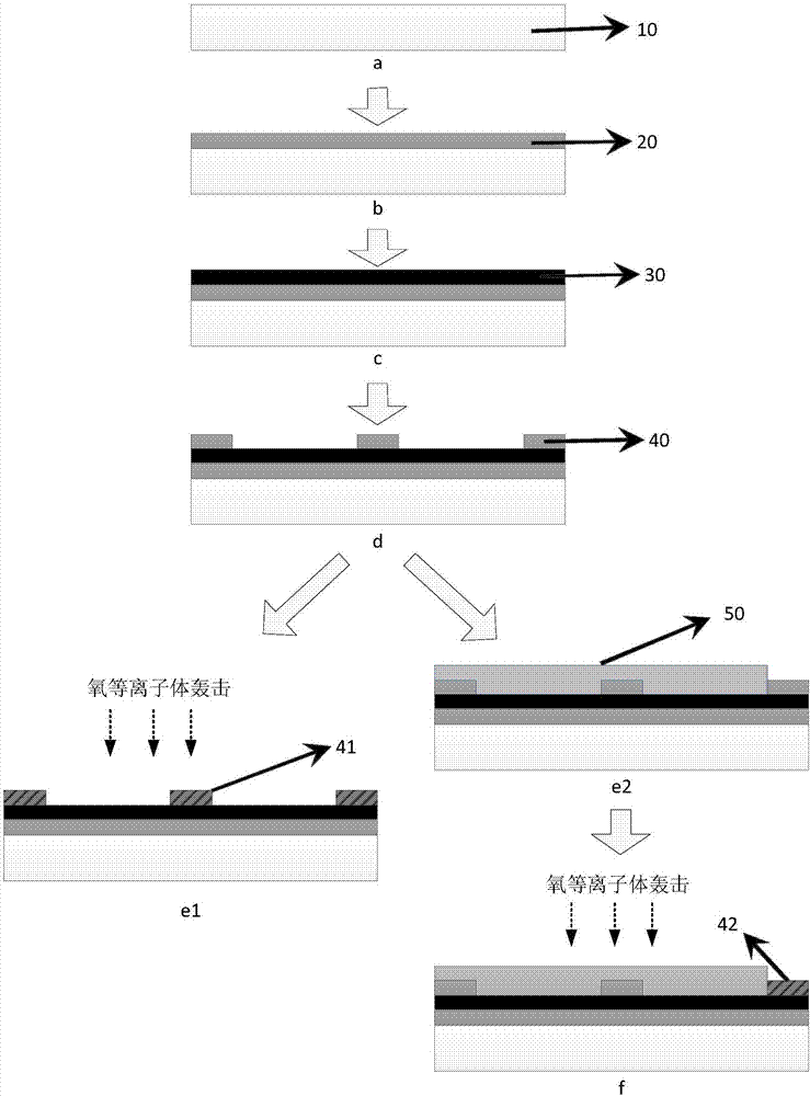
[0039] A tunable metamaterial structure based on variable surface resistance, including a metal thin film bottom layer 20, an intermediate dielectric layer 30, and a patterned metal thin film top layer 40 with adjustable square resistance. The preparation steps of the above-mentioned tunable metamaterial structure based on all variable surface resistance are as follows:

[0040] S1: Prepare the substrate 10.

[0041] S2: The metal thin film bottom layer 20 is prepared by magnetron sputtering. The material of the metal thin film bottom layer 20 is titanium, and the thickness of the metal thin film bottom layer 20 is 100nm-500nm. During the preparation process, the sputtering power is 50-250W, and the pressure of the reaction chamber is It is 1-10Pa, and the sputtering time is 10-30 minutes.

[0042] S3: Prepare the intermediate medium layer 30 by spin coating, the material of the intermediate medium layer 30 is PI, during the preparation process, the forward rotation speed is ...

Embodiment 2

[0046] A tunable metamaterial structure based on variable surface resistance, including a metal thin film bottom layer 20, an intermediate dielectric layer 30, a patterned metal thin film top layer 40 and a dielectric protection layer 50 with adjustable partial square resistance.

[0047] The above-mentioned method for preparing a tunable metamaterial structure based on partially variable surface resistance, the steps are as follows:

[0048] S1: Prepare the substrate 10.

[0049] S2: The metal thin film bottom layer 20 is prepared by magnetron sputtering. The material of the metal thin film bottom layer 20 is titanium, and the thickness of the metal thin film bottom layer is 100nm-500nm. During the preparation process, the sputtering power is 50-250W, and the pressure in the reaction chamber is 1-10Pa, sputtering time is 10-30 minutes.

[0050] S3: Prepare the intermediate medium layer 30 by spin coating, the material of the intermediate medium layer 30 is PI, and the forwar...

Embodiment 3

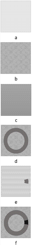
[0056] Such as figure 2 A tunable resonant ring metamaterial structure based on variable surface resistance and its preparation method are shown.

[0057] Prepare the underlying metal film by magnetron sputtering, adjust the process parameters, and control the thickness of the metal film to 400nm, such as figure 2 As shown in a; the intermediate silicon nitride dielectric layer is prepared by PECVD, and the thickness of the dielectric film is controlled to be 4.5 μm, such as figure 2 Shown in b; adopt magnetron sputtering method to prepare top layer metal thin film, adjust process parameter, control metal thin film thickness is 100nm, as figure 2 As shown in c; photolithography and reactive ion etching are used to pattern the top metal film, and the active etchant in the etching gas is BCl 3 and Cl 2 ;Neutral gas N 2 , set BCl 3 , Cl 2 , N 2 The flow ratio is 1:2:1, the RF power is 150W, and the reaction chamber pressure is 3Pa. Controlling the reactive ion etching ...


PUM

PropertyMeasurementUnit
Thicknessaaaaaaaaaa
Thicknessaaaaaaaaaa
Thicknessaaaaaaaaaa

Abstract

The invention discloses a tunable metamaterial structure based on variable surface square resistance and a manufacturing method thereof, which are applied in the fields of modulators, detectors and the like of infrared and Terahertz bands. The manufacturing method of the tunable metamaterial structure comprises: manufacturing a three-layer metamaterial structure having a graphic metal film at the top, and then bombarding the metamaterial structure by adopting oxygen plasma to control the surface square resistance of the top metal film, thus obtaining the tunable metamaterial structure. Before bombarding of the oxygen plasma, the dielectric film covers the top metal film to selectively control the square resistance of a part of the top metal film, thus modulating the resonance peak frequency of a metamaterial and the like. The tunable metamaterial structure is simple in manufacturing process and tuning manner, is compatible with an MEMS process and obvious in infrared and Terahertz band modulation effect, and has a broad application prospect.

Description

technical field [0001] The invention relates to the fields of modulators and detectors in the infrared and terahertz bands, and in particular to a structure of a tunable metamaterial based on variable surface resistance and a preparation method thereof. Background technique [0002] Infrared is an electromagnetic wave with a wavelength between microwaves and visible light, and a non-visible light with a wavelength between 760nm and 1mm that is longer than red light. Terahertz (THz) waves refer to electromagnetic radiation with a frequency between 0.1-10 THz (wavelength 30 μm-3 mm). Due to the unique advantages of THz electromagnetic radiation, such as transient, broadband, low-energy, and penetrating properties, terahertz imaging technology has great application value in the fields of object imaging, environmental monitoring, medical diagnosis, radio astronomy, and broadband mobile communications. . Infrared microbolometer based on microbridge structure, as the mainstream ...

Claims


Application Information

Patent Timeline
IPC IPC(8): G02B1/00G03F7/00
CPCG02B1/002G03F7/0005
Inventor 苟君梁恺牛青辰王军蒋亚东
Owner UNIV OF ELECTRONIC SCI & TECH OF CHINA
Why Eureka
Try Eureka