
Pre-impregnated material for circuit board, laminated board, preparation method and printed circuit board comprising pre-impregnated material

A technology for printed circuit boards and circuit substrates, applied in the direction of circuit substrate materials, printed circuits, printed circuits, etc., can solve the problem of narrowing the selection range of reinforcing materials and resins, and achieve the effect of solving design difficulties

Active Publication Date: 2017-08-18
GUANGDONG SHENGYI SCI TECH
View PDF6 Cites 6 Cited by
  • Summary
  • Abstract
  • Description
  • Claims
  • Application Information

AI Technical Summary

Problems solved by technology

The method is limited by the Dk of the reinforcing material, resulting in a narrower selection of reinforcing materials and resins

Method used


Image

  • Pre-impregnated material for circuit board, laminated board, preparation method and printed circuit board comprising pre-impregnated material
  • Pre-impregnated material for circuit board, laminated board, preparation method and printed circuit board comprising pre-impregnated material
  • Pre-impregnated material for circuit board, laminated board, preparation method and printed circuit board comprising pre-impregnated material

Examples


Embodiment 1

[0117] (1) Take a suitable container, add a total of 100 parts by mass of polyphenylene ether resin with acryloyl modified groups at both ends and dicumyl peroxide, then add 1 to 20 parts by mass of fused silica, and then add An appropriate amount of solvent is stirred for a certain period of time to form the first glue solution (polyphenylene ether resin system); then NE-type 1080 glass fiber cloth is dipped in the glue solution, and then the solvent is dried to obtain a prepreg core material layer; Dielectric constant Dk of prepreg core layer after heat treatment 芯 3.6, thickness H 芯 50μm; at Dk 芯 and H 芯 To design a laminate for a given situation, its Dk is required 层压板 It is about 3.3, and the thickness is about 400μm:

[0118] (2) Select the polyphenylene ether resin system as the second glue solution; take a suitable container, add a total of 100 parts by mass of polyphenylene ether resin and dicumyl peroxide whose two terminal modification groups are acryloyl groups...

Embodiment 2

[0123] (1) Take a suitable container, add a total of 100 parts by mass of polyphenylene ether resin with acryloyl modified groups at both ends and dicumyl peroxide, then add 1 to 20 parts by mass of fused silica, and then add An appropriate amount of solvent is stirred for a certain period of time to form the first glue solution (polyphenylene ether resin system); then NE-type 1080 glass fiber cloth is dipped in the glue solution, and then the solvent is dried to obtain a prepreg core material layer; Dielectric constant Dk of prepreg core layer after heat treatment 芯 3.6, thickness H 芯 50μm; at Dk 芯 and H 芯 To design a laminate for a given situation, its Dk is required 层压板 It is about 3.75, and the thickness is about 400μm:

[0124] (2) Select the epoxy resin system as the second glue solution; get a suitable container, add a total of 100 parts by mass of Dicy of low bromine bisphenol A type epoxy resin and suitable equivalent ratio, an appropriate amount of solvent, stir ...

Embodiment 3

[0129] (1) Take a suitable container, add a total of 100 parts by mass of polyphenylene ether resin with acryloyl modified groups at both ends and dicumyl peroxide, then add 1 to 20 parts by mass of fused silica, and then add An appropriate amount of solvent is stirred for a certain period of time to form the first glue solution (polyphenylene ether resin system); then NE-type 1080 glass fiber cloth is dipped in the glue solution, and then the solvent is dried to obtain a prepreg core material layer; Dielectric constant Dk of prepreg core layer after heat treatment 芯 3.6, thickness H 芯 50μm; at Dk 芯 and H 芯 To design a laminate for a given situation, its Dk is required 层压板 It is about 3.2, and the thickness is about 450 μm:

[0130] (2) Select the polyphenylene ether resin system as the second glue solution; take a suitable container, add a total of 100 parts by mass of polyphenylene ether resin and dicumyl peroxide whose two terminal modification groups are acryloyl group...


PUM

PropertyMeasurementUnit
thicknessaaaaaaaaaa
thicknessaaaaaaaaaa
thicknessaaaaaaaaaa

Abstract

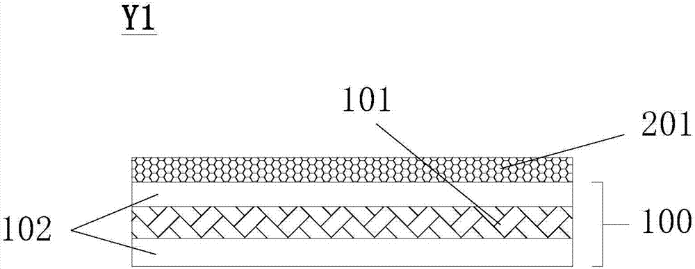
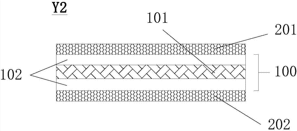
The invention relates to a pre-impregnated material for a circuit board. The pre-impregnated material comprises a pre-impregnated core material layer and an outer resin layer formed on at least one side of the pre-impregnated core material layer, wherein the pre-impregnated core material layer comprises a reinforcing material and an inner resin layer coating the outer side of the reinforcing material; the dielectric constant of the outer resin layer is denoted as Dk<outside> and the thickness is denoted as H<outside>; the dielectric constant of the pre-impregnated core material layer is denoted as Dk<core> and the thickness is denoted as H<core>; and the dielectric constant Dk<laminated board> of the laminated board meets the condition as follows: Dk< pre-impregnated material>=(Dk<core>*H<core>+Dk<outside>*H<outside>) / (H<core>+H<outside>). The Dk value of the laminated board is calculated according to weight of the thickness and the differences between the pre-impregnated core material layer and the outer resin layer in Dk and thickness, the design problem of the Dk of the laminated board is achieved, the design range of the Dk of the laminated board is not limited to Dk of the reinforcing material, and the problem that a PCB is difficult to design is solved.

Description

technical field [0001] The invention belongs to the technical field of electronic materials, and in particular relates to a prepreg for circuit substrates, a laminate, a preparation method and a printed circuit board containing the same. The dielectric constant Dk value of the prepreg and the laminate can be design. Background technique [0002] At present, the manufacturing process of the laminate is mainly as follows: the reinforcing material impregnated with the resin composition is baked and dried, so that the resin composition becomes a prepreg with a certain degree of curing from the uncured glue, and then the prepreg is Prepreg slices are made into prepreg sheets, and then one or more prepreg sheets are laminated together, and one side / both sides are covered with copper foil or release film, using a high temperature press machine, after heating, adding Pressed to make a laminate, it is mainly used in the production of printed circuit boards (PCB). The manufacturing ...

Claims


Application Information

Patent Timeline
Patent Type & Authority Applications(China)
IPC IPC(8): C08J5/24C08L63/00C08L79/04C08L71/12C08K3/36C08K7/14B32B27/28B32B27/38B32B27/06B32B15/08B32B15/092B32B15/20B32B17/02B32B17/10H05K1/03
CPCH05K1/036H05K1/0366C08K3/36C08K7/14C08L63/00C08L71/126C08L79/04B32B5/02B32B15/08B32B15/092B32B15/20B32B17/02B32B17/10B32B27/06B32B27/12B32B27/28B32B27/285B32B27/38H05K2201/029C08L2205/03B32B2262/101B32B2457/08C08J5/249C08J5/244
Inventor 陈虎
Owner GUANGDONG SHENGYI SCI TECH
Learn More