Silicon-carbon negative electrode material and preparation method thereof
A negative electrode material, silicon carbon technology, applied in the field of silicon carbon negative electrode materials and its preparation, can solve the problems affecting the effect of graphene, the weak force of graphene sheets, and the impact on the capacity of silicon-based materials, etc., to achieve excellent cycle performance, Minimized hindrance and excellent effect of volume change
- Summary
- Abstract
- Description
- Claims
- Application Information
AI Technical Summary
Problems solved by technology
Method used
Image
Examples
Embodiment 1
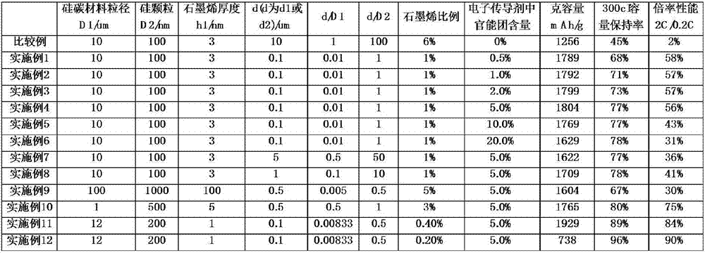
[0035] Embodiment 1 differs from Comparative Example 1 in that the present embodiment comprises the following steps:
[0036] Step 1, select the silicon particle that particle diameter is 100nm, the functionalized graphene sheet layer that sheet thickness is 3nm, sheet plane diameter is 0.1 μm is electronic conduction component (mass ratio between silicon particle and graphene is 99%) : 1); the functional group (including hydroxyl, carboxyl and carbonyl) content is 0.5% of the mass of the entire electron-conducting component, and the precursor is obtained after being uniformly mixed with a solvent;
[0037] Step 2, through the hydrothermal reaction, the graphene molecules of the electron-conducting components containing functional groups are cross-linked to form a strong bonding force to complete the construction of the conductive network, and at the same time fix the primary particles in the network structure; Through mechanical shearing (stirring), a structure in which prima...
Embodiment 2
[0040] Embodiment 2 is different from Embodiment 1 in that this embodiment includes the following steps:
[0041] Step 1, select the silicon particle that particle diameter is 100nm, the functionalized graphene sheet layer that sheet thickness is 3nm, sheet plane diameter is 0.1 μm is electronic conduction component (mass ratio between silicon particle and graphene is 99%) : 1); the functional group (including hydroxyl, carboxyl and carbonyl) content is 1% of the mass of the entire electron-conducting component, and the precursor is obtained after being uniformly mixed with a solvent;
[0042] Others are the same as in Example 1, and will not be repeated here.
Embodiment 3
[0043] Embodiment 3 is different from Embodiment 1 in that this embodiment includes the following steps:
[0044] Step 1, select the silicon particle that particle diameter is 100nm, the functionalized graphene sheet layer that sheet thickness is 3nm, sheet plane diameter is 0.1 μm is electronic conduction component (mass ratio between silicon particle and graphene is 99%) : 1); the functional group (including hydroxyl, carboxyl and carbonyl) content is 2% of the mass of the entire electron-conducting component, which is uniformly mixed with a solvent to obtain a precursor;
[0045] Others are the same as in Example 1, and will not be repeated here.
PUM
| Property | Measurement | Unit |
|---|---|---|
| diameter | aaaaa | aaaaa |
| thickness | aaaaa | aaaaa |
| diameter | aaaaa | aaaaa |
Abstract
Description
Claims
Application Information
