Composite hole transport layer with multi-layer periodic doping structure, LED device structure and application and preparation method of LED device structure

A technology of hole transport layer and LED device, applied in semiconductor/solid-state device manufacturing, electric solid-state device, semiconductor device, etc., can solve the problems of unbalanced carrier injection, high color purity, narrow half-peak width, etc., and achieve improved Hole injection ability, high color purity, effect of improving injection balance

Active Publication Date: 2017-08-29
SHANGHAI UNIV
View PDF5 Cites 26 Cited by
  • Summary
  • Abstract
  • Description
  • Claims
  • Application Information

AI Technical Summary

Problems solved by technology

[0002] Inorganic new quantum dot luminescent material has the advantages of continuously adjustable luminescent spectrum, narrow half-peak width, high color purity, low cost, high stability, etc. Its quantum dot electroluminescent device has broad development prospects, but for the previously reported The quantum dot device structure, due to its relatively large hole relative to the electron injection barrier, leads to unbalanced carrier injection, and the electron leakage current will cause fluorescence quenching of QDs, which leads to an increase in the device's turn-on voltage and fluorescence efficiency. space
Due to the limitation of the work function of quantum dots in existing LED devices, the problem of carrier injection imbalance has become an urgent technical problem to be solved.

Method used


Image

  • Composite hole transport layer with multi-layer periodic doping structure, LED device structure and application and preparation method of LED device structure
  • Composite hole transport layer with multi-layer periodic doping structure, LED device structure and application and preparation method of LED device structure
  • Composite hole transport layer with multi-layer periodic doping structure, LED device structure and application and preparation method of LED device structure

Examples


Embodiment 1

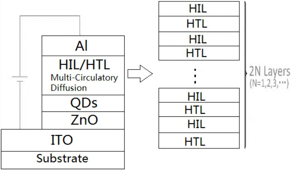
[0030] In this embodiment, see figure 1 , A composite hole transport layer with a multilayer periodic doping structure, the composite hole transport layer has a multilayer composite structure, and the composite hole transport layer is made of MoO 3 Inorganic materials are used as doping materials. The composite hole transport layer is composed of N layers of doped organic layered structural units sequentially stacked, N=10, and each layer of doped organic layered structural units consists of a hole transport layer and doped materials The layer composition is such that a doped material layer is arranged between any adjacent hole transport layers as a hole injection layer to form a 10-period sequence with the combination of this doped material layer and CBP hole transport layer as a structural unit A 20-layer composite hole transport layer structure, in which the first hole transport layer and the first hole injection layer constitute the first doped organic layered structural unit...

Embodiment 2

[0057] This embodiment is basically the same as the first embodiment, and the special features are:

[0058] In this embodiment, a method for manufacturing the LED device structure of this embodiment includes the following steps:

[0059] a. This step is the same as the first embodiment;

[0060] b. This step is the same as the first embodiment;

[0061] c. This step is the same as the first embodiment;

[0062] d. Then transfer the substrate assembly with the light-emitting layer prepared in the step c to the cavity of the thermal evaporation device, and control the cavity pressure of the thermal evaporation device to be not higher than 2×10 -4 Pa, then adjust the temperature of the evaporation heat source so that the evaporation source medicine reaches the sublimation point, and the evaporation source medicine is deposited on the surface of the light-emitting layer in a gas state to form a composite hole transport layer capable of solid-gas-solid three-phase conversion , The composit...

Embodiment 3

[0069] This embodiment is basically the same as the previous embodiment, and the special features are:

[0070] In this embodiment, a method for manufacturing the LED device structure of this embodiment includes the following steps:

[0071] a. This step is the same as the first embodiment;

[0072] b. This step is the same as the first embodiment;

[0073] c. This step is the same as the first embodiment;

[0074] d. Then transfer the substrate assembly with the light-emitting layer prepared in the step c to the cavity of the thermal evaporation device, and control the cavity pressure of the thermal evaporation device to be not higher than 2×10 -4 Pa, then adjust the temperature of the evaporation heat source to make the evaporation source medicine reach the sublimation point, and deposit the evaporation source medicine in a gas state on the surface of the light-emitting layer to form a composite hole transport layer capable of solid-gas-solid three-phase conversion , The composite ho...


PUM


Abstract

The invention discloses a composite hole transport layer with a multi-layer periodic doping structure, an LED device structure and application and preparation method of the LED device structure. By doping a metal oxide material in a hole organic transport layer of a quantum-dot light emitting device, the hole transport layer (HTL) taking the doping organic layer as a structural unit and with multi-layer periodic doping is fabricated, the hole injection capability of the device is remarkably improved, so that the carrier injection balance in the device is improved. Meanwhile, the influence of the doping proportion of the metal oxide doping material in the HTL on the light emitting property of the device is symmetrically researched. The structure is not limited to a quantum-dot LED, and the device structure can be implanted to other types of photoelectric devices.

Description

Technical field [0001] The invention relates to a functional layer, device, application and preparation method of a semiconductor light-emitting device, in particular to a composite doped hole transport layer, an LED device structure, application and preparation method, and is applied to the technical field of LED devices. Background technique [0002] The new inorganic quantum dot luminescent material has the advantages of continuously adjustable luminescence spectrum, narrow half-maximum width, high color purity, low cost, and high stability. Its quantum dot electroluminescent device has broad development prospects, but for the previously reported In the structure of quantum dot devices, due to the relatively large hole relative to the electron injection barrier, the carrier injection is unbalanced, and the electron leakage current will cause fluorescence quenching of QDs, etc., which leads to an increase in the switching voltage and fluorescence efficiency of the device. space...

Claims


Application Information

Patent Timeline
Patent Type & Authority Applications(China)
IPC IPC(8): H01L51/50H01L51/56
CPCH10K71/164H10K50/115H10K50/155H10K50/156H10K50/17H10K71/00Y02E10/549
Inventor 杨绪勇黄霏张建华申飘阳
Owner SHANGHAI UNIV
Why Eureka
Try Eureka