

Organic insulating layer-based gradient-doped IGZO thin-film transistor and preparation method thereof
A technology of organic insulating layer and thin film transistor, which is applied in the field of electronics, can solve the problems of organic insulating layer damage, lattice mismatch, large leakage current, etc., and achieve the effects of reducing damage, reducing defects, and solving biological pollution
- Summary
- Abstract
- Description
- Claims
- Application Information
AI Technical Summary
Problems solved by technology
Method used
Image

Examples
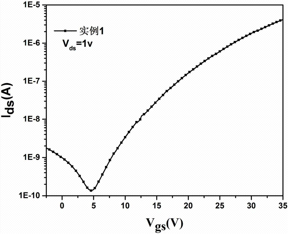
Embodiment 1
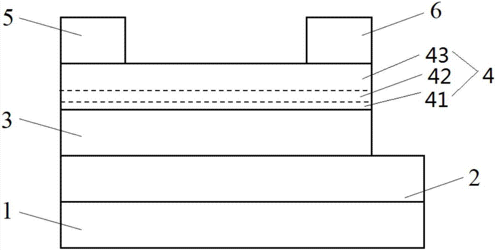
[0030] A gradient doped IGZO thin film transistor based on an organic insulating layer, characterized in that it includes a substrate 1, a gate electrode 2, an organic insulating layer 3, a gradient doped IGZO semiconductor layer 4, and a gradient doped IGZO layer arranged in sequence from bottom to top. A source electrode 5 and a drain electrode 6 are juxtaposed on the semiconductor layer 4 , wherein the gradient doped IGZO semiconductor layer 3 includes the lowermost IGZO film 41 , the uppermost IGZO film 43 , and the middle layer IGZO film 42 with increasing concentrations in sequence.
[0031] Specifically, the material of the substrate 1 is glass; the material of the gate electrode 2 is indium tin oxide, and the thickness of the gate electrode 2 is 200 nm; the material of the organic insulating layer 3 is polymethyl methacrylate, and the thickness is 200 nm; the gradient doping In the IGZO semiconductor layer 4, the oxygen partial pressure of the lowermost IGZO thin film 4...
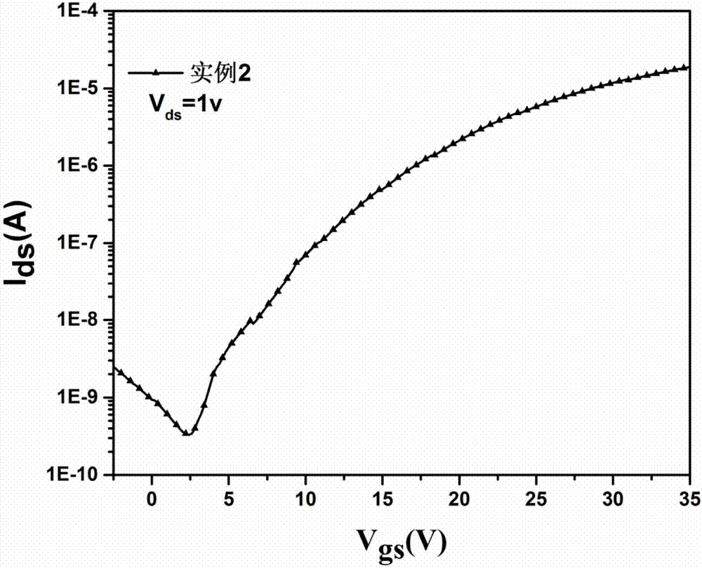
Embodiment 2
[0040] A gradient doped IGZO thin film transistor based on an organic insulating layer, characterized in that it includes a substrate 1, a gate electrode 2, an organic insulating layer 3, a gradient doped IGZO semiconductor layer 4, and a gradient doped IGZO layer arranged in sequence from bottom to top. A source electrode 5 and a drain electrode 6 are juxtaposed on the semiconductor layer 4 , wherein the gradient doped IGZO semiconductor layer 3 includes the lowermost IGZO film 41 , the uppermost IGZO film 43 , and the middle layer IGZO film 42 with increasing concentrations in sequence.
[0041] Specifically, the material of the substrate 1 is glass; the material of the gate electrode 2 is indium tin oxide, and the thickness of the gate electrode 2 is 200nm; the material of the organic insulating layer 3 is polyvinyl alcohol, and the thickness is 200nm; the gradient doped IGZO semiconductor layer In 4, the oxygen partial pressure of the lowermost IGZO film 41 is 4%, the thick...
PUM
 Abstract
Description
Claims
Application Information