Method for building CsPbBr3 nanosheet electroluminescent device by chemical vapor deposition (CVD)
An electroluminescent device and nanosheet technology, which is applied to electrical components, semiconductor devices, circuits, etc., can solve the problems of difficult realization of devices and failure to realize single nanostructure electrolysis, and achieve the effect of simple process technology and convenient control.
- Summary
- Abstract
- Description
- Claims
- Application Information
AI Technical Summary
Problems solved by technology
Method used
Image
Examples
Embodiment 1
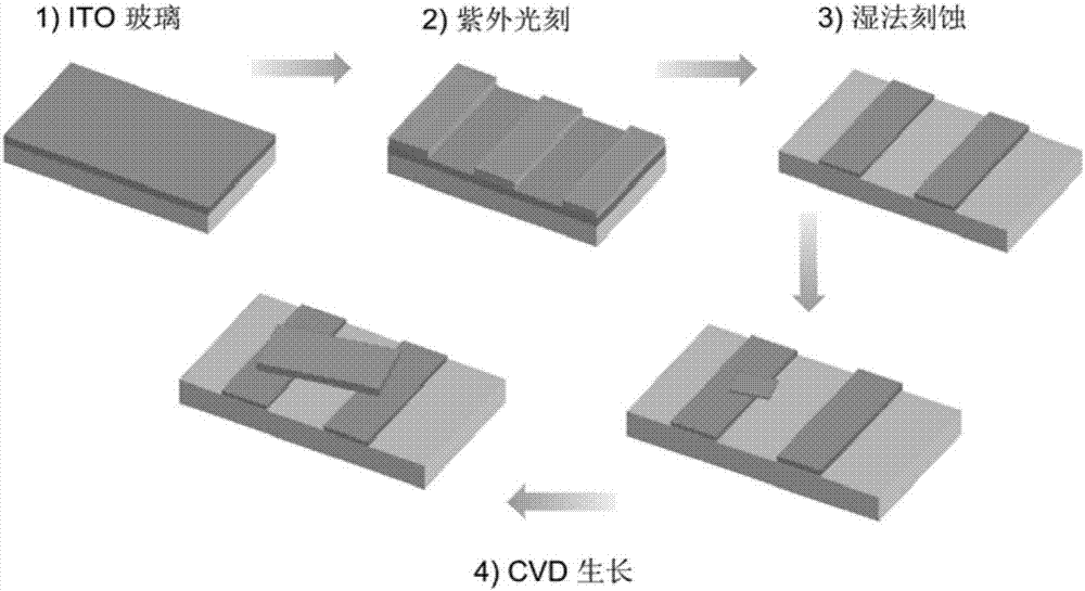
[0051] Take the ITO sheet as the substrate, cut it into 15mm×15mm size, wash it ultrasonically in acetone and ethanol solution for 15min respectively, take it out and dry it on a heating table at 120°C. The ITO glass substrate is placed on a high-speed rotary machine, and a layer of 600nm thick photoresist (negative glue) is spin-coated at 2500 / min and time 60s. Pre-baking, temperature 120°C, time 90s. Expose for 10s with a reticle mask, and each electrode of the designed pattern is independent of each other. Post-bake at 120°C for 90s. Then develop, time 20s. After hardening the film on a heating platform at 150°C for 5 minutes, put it into the ITO etching solution for 15 minutes to obtain the ITO electrode with the desired pattern. Wash the ITO glass with electrodes ultrasonically in acetone and ethanol solutions for 15 minutes, take it out and dry it in an oven at 60°C for the next step of CVD growth. The spacing between adjacent electrodes is 10 microns.
[0052] CsBr...
Embodiment 2
[0054] Take the ITO sheet as the substrate, cut it into 15mm×15mm size, wash it ultrasonically in acetone and ethanol solution for 15min respectively, take it out and dry it on a heating table at 120°C. The ITO glass substrate is placed on a high-speed rotary machine, and a layer of 600nm thick photoresist (negative glue) is spin-coated at 2500 / min and time 60s. Pre-baking, temperature 120°C, time 90s. Expose for 10s with a reticle mask, and the designed pattern is an interdigital electrode. Post-bake at 120°C for 90s. Then develop, time 20s. After hardening the film on a heating platform at 150°C for 5 minutes, put it into the ITO etching solution for 15 minutes to obtain the ITO electrode with the desired pattern. The ITO glass engraved with electrodes was ultrasonically washed in acetone and ethanol solutions for 15 minutes, and then taken out and dried in an oven at 60°C for the next step of CVD growth. The spacing between adjacent electrodes is 5 microns.
[0055] Cs...
PUM
 Abstract
Description
Claims
Application Information


