Piezoresistive pressure sensor applicable to surface mounting process and manufacturing method thereof

A pressure sensor and manufacturing method technology, applied in the sensor field, can solve the problems affecting device performance, failure to realize pressure sensor processing, residual stress, etc., and achieve the effects of improving selectivity, reducing equipment investment and processing costs, and reducing processing costs.

Active Publication Date: 2017-09-19
GUANGDONG HEWEI INTEGRATED CIRCUIT TECH
View PDF8 Cites 4 Cited by
  • Summary
  • Abstract
  • Description
  • Claims
  • Application Information

AI Technical Summary

Problems solved by technology

However, this method does not realize the processing of pressure sensors that are convenient for 3D packaging at the wafer level; in addition, through-holes are processed through TSV technology in the packaging stage, and metal is plated in the through-holes, because the thermal expansion coefficients of metal and semiconductor materials do not match. Generate residual stress and affect device performance

Method used


Image

  • Piezoresistive pressure sensor applicable to surface mounting process and manufacturing method thereof
  • Piezoresistive pressure sensor applicable to surface mounting process and manufacturing method thereof
  • Piezoresistive pressure sensor applicable to surface mounting process and manufacturing method thereof

Examples


Embodiment Construction

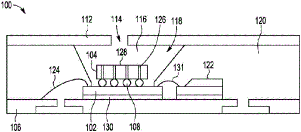
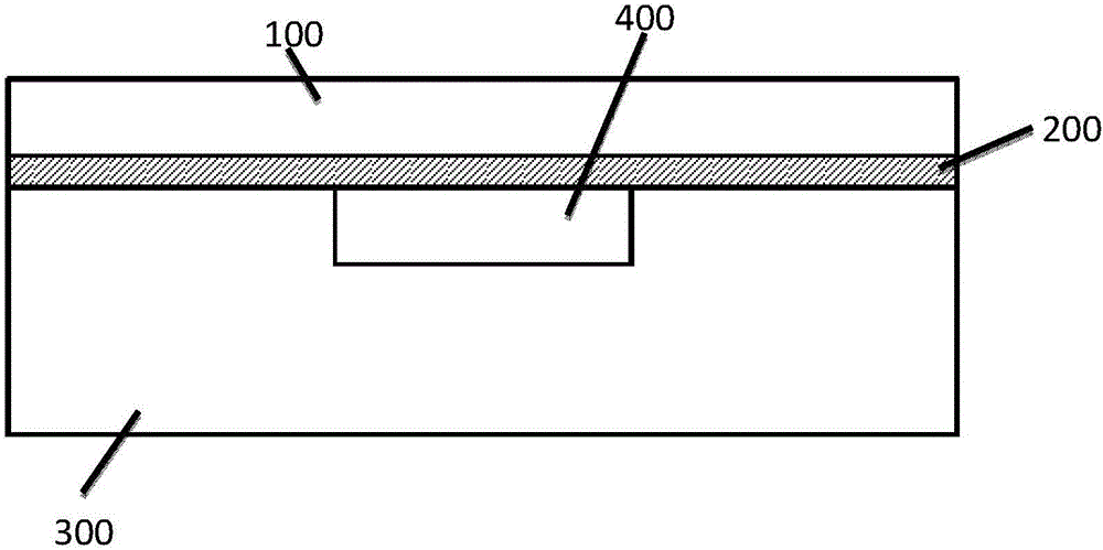
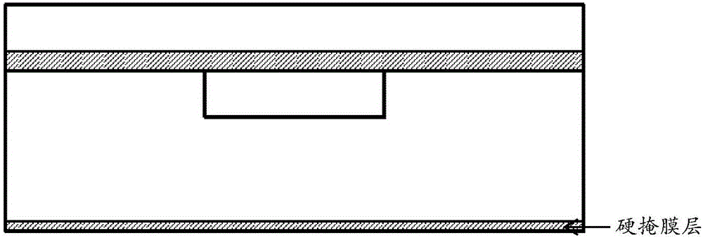
[0057] The embodiment of the present invention is based on a silicon (Cavity-SOI) wafer on a prefabricated cavity insulating substrate, and the wafer structure is as follows figure 2 As shown, the wafer includes a silicon substrate 300 , an insulating layer 200 (silicon dioxide), and a top layer of silicon 100 ; The doping concentration and crystal orientation of the top-layer silicon 100 and the substrate silicon 300 can be freely selected according to actual needs, but the doping of the top-layer silicon 100 and the substrate silicon 300 must be opposite. The embodiment of the present invention only lists a typical application: both the top layer silicon 100 and the substrate silicon 300 adopt the (100) crystal orientation, the top layer silicon is N-type doped, and the substrate silicon is P-type doped (of course, it can also be the top layer Silicon is P-type doped, substrate silicon is N-type doped).

[0058] The relevant implementation steps can be as follows:

[0059...


PUM


Abstract

The invention relates to a piezoresistive pressure sensor applicable to a surface mounting process and a manufacturing method thereof. A utilized wafer structure comprises a substrate semiconductor material, a top-layer semiconductor material and an insulating layer, wherein a cavity is formed in an interface position of the insulating layer in the substrate semiconductor material; the top-layer semiconductor material and the substrate semiconductor material are formed by inverse-phase doping; the substrate semiconductor material is provided with an electric isolation groove; an electric contact hole is formed in the substrate semiconductor material surrounded by the electric isolation groove; metal is re-doped and deposited into the electric contact hole to form an electric channel and a metal pin; a piezoresistive strip, an electric lead wire region and an electric connection hole of the pressure sensor are formed in the top-layer semiconductor material; the electric lead wire region is overlapped with the substrate semiconductor material surrounded by one part of the piezoresistive strip and the electric isolation groove; the electric connection hole is located in an overlapped region of the electric lead wire region and the substrate semiconductor material; and an electric connection channel is formed by depositing a conductive layer in the electric connection hole. By adopting the piezoresistive pressure sensor provided by the invention, three dimension (3D) packaging with a corresponding control circuit (IC) is conveniently and subsequently realized, and the cost is low.

Description

technical field [0001] The invention relates to the technical field of sensors, in particular to a piezoresistive pressure sensor suitable for surface mount technology and a manufacturing method thereof. Background technique [0002] With the rise of industries such as the Internet of Things, MEMS (Micro electro Mechanical Systems) sensors have great application prospects due to their small size, low power consumption, light weight, and fast response. In particular, MEMS pressure sensors have huge applications in automotive electronics, consumer products, industrial control and other fields. [0003] At present, MEMS sensors need to be used together with the corresponding control IC to achieve specific functions. The MEMS sensor and the corresponding control IC are packaged in a package module. There are currently two ways: (1) Put the MEMS sensor and the corresponding control IC side by side On a packaging substrate, the electrical connection between the MEMS sensor and th...

Claims


Application Information

Patent Timeline
Patent Type & Authority Applications(China)
IPC IPC(8): B81B7/02B81C1/00G01L1/18
CPCB81B7/02B81C1/00095B81C1/00301G01L1/18
Inventor 周志健朱二辉陈磊杨力建于洋邝国华
Owner GUANGDONG HEWEI INTEGRATED CIRCUIT TECH
Why Eureka
Try Eureka