InAs/AlSb HEMT and MOS-HEMT device manufacturing methods

A device and deposition technology, applied in the field of microelectronics, can solve problems such as device gate leakage, achieve the effect of reducing series resistance and gate current leakage

Active Publication Date: 2017-09-22
XIDIAN UNIV
View PDF2 Cites 1 Cited by
  • Summary
  • Abstract
  • Description
  • Claims
  • Application Information

AI Technical Summary

Problems solved by technology

[0005] The object of the present invention is to provide a kind of preparation method of InAs/AlSb HEMT device, provide a kind of preparatio

Method used


Image

  • InAs/AlSb HEMT and MOS-HEMT device manufacturing methods
  • InAs/AlSb HEMT and MOS-HEMT device manufacturing methods
  • InAs/AlSb HEMT and MOS-HEMT device manufacturing methods

Examples


Embodiment 1

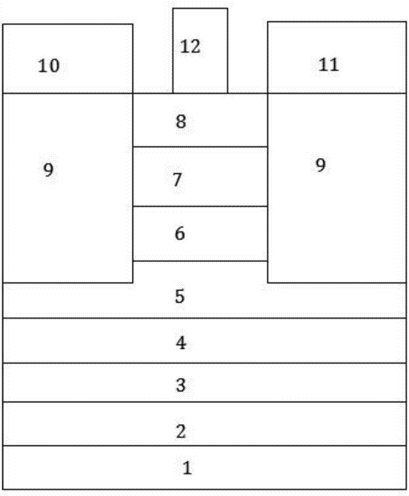
[0081] The InAs / AlSb HEMT device prepared in this embodiment uses GaAs as the substrate, the buffer layer 2 is AlGaSb, and the doped layer 6 is doped with a Si concentration of 4*10 19 cm -3 InAs layer. Concrete preparation process is as follows:

[0082] Step 1, epitaxial material growth: Using MBE process, grow buffer layer 2 (buffer layer 2 is AlGaSb), AlSb lower barrier layer 3, InAs channel layer 4, AlSb isolation layer 5, InAs doped Layer 6, AlSb upper barrier layer 7, InAlAs hole blocking layer 8;

[0083] Step 2. Countertop isolation:

[0084] (a) cleaning the epitaxially grown InAs / AlSb material, and then blowing it dry with nitrogen;

[0085] (b) Perform photolithography and etching on the cleaned InAs / AlSb material to complete the mesa isolation of the epitaxial material;

[0086] Step 3. Preparation of ohmic contacts:

[0087] (a) Clean the InAs / AlSb material after the table isolation, and then dry it with nitrogen;

[0088] (b) performing photolithography o...

Embodiment 2

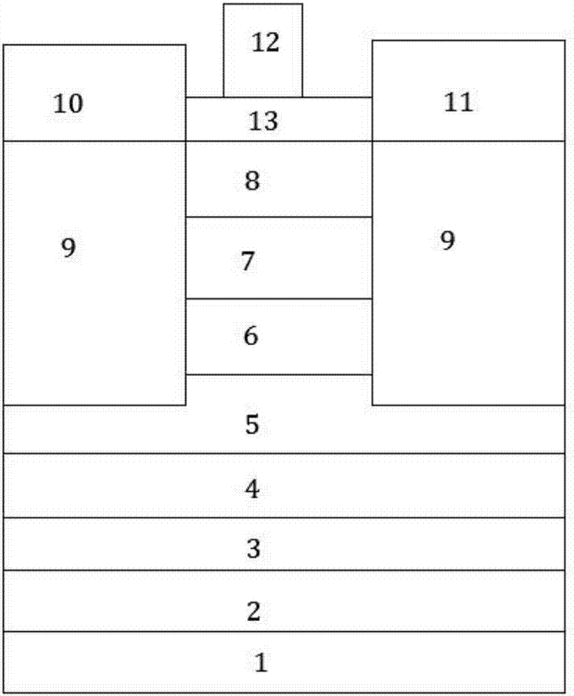
[0110] The InAs / AlSb MOS-HEMT device prepared in this embodiment uses GaAs as the substrate, the buffer layer 2 is AlGaSb, and the doped layer 6 is doped with a Si concentration of 4*10 19 cm -3 InAs layer, dielectric layer 13 is HfO 2 . Concrete preparation process is as follows:

[0111] 1) Epitaxial material growth: Using MBEMOCVD process, grow buffer layer 2 (buffer layer 2 is AlGaSb), AlSb lower barrier layer 3, InAs channel layer 4, AlSb isolation layer 5, doped layer 6 on substrate 1 in sequence , AlSb upper potential barrier layer 7, InAlAs hole blocking layer 8;

[0112] 2) Countertop isolation:

[0113] (a) cleaning the epitaxially grown InAs / AlSb material, and then blowing it dry with nitrogen;

[0114] (b) Photolithography and etching are performed on the cleaned InAs / AlSb material to complete the mesa isolation of the epitaxial material.

[0115] 3) Preparation of ohmic contacts:

[0116] (a) Clean the InAs / AlSb material after the table isolation, and then ...


PUM


Abstract

The invention discloses InAs/AlSb HEMT and MOS-HEMT device manufacturing methods, mainly to reduce on-state resistance of a device and solve the problem of gate current leakage. The InAs/AlSb HEMT device manufacturing method comprises the following process steps of: 1) epitaxial material growth, 2) mesa isolation, 3) ohmic contact manufacturing, 4) schottky gate contact manufacturing, 5) Pad deposition and 6) passivation. The InAs/AlSb MOS-HEMT device manufacturing method comprises the following process steps of: 1) epitaxial material growth, 2) mesa isolation, 3) ohmic contact manufacturing, 4) insulated gate manufacturing, 5) Pad deposition and 6) passivation. A gate slot etching step is saved, the gate current leakage is reduced, and the on-state resistance of the device is also reduced.

Description

technical field [0001] The invention belongs to the technical field of microelectronics, and relates to a method for preparing InAs / AlSb HEMT and MOS-HEMT devices, which can be used for the preparation of high-speed, low-power InAs / AlSb HEMT or MOS-HEMT devices. Background technique [0002] In today's era, microelectronic technology is developing rapidly, and its application has penetrated into various fields of the national economy. In order to further meet the requirements of high-speed, low power consumption and low-noise device performance, new device structures have also emerged as the times require. From MOS devices to HEMT devices and MOS-HEMT structures. Among them, InAs / AlSb HEMT and MOS-HEMT device structures are favored due to their high carrier mobility, high saturation drift velocity, low critical saturation electric field, strong radiation resistance, fast speed, low power consumption and low noise. [0003] The manufacture of InAs / AlSb HEMT or MOS-HEMT devic...

Claims


Application Information

Patent Timeline
IPC IPC(8): H01L21/335H01L21/28
CPCH01L29/401H01L29/66462
Inventor 吕红亮张静杨施政张义门张玉明
Owner XIDIAN UNIV
Why Eureka
Try Eureka