Laser machining method and device for wafer

A laser processing and wafer technology, applied in metal processing, laser welding equipment, metal processing equipment, etc., can solve the problems of laser beam energy loss, Low-K layer peeling, increasing laser energy, etc., and achieve energy control accuracy High, easy to prepare, and the effect of improving the light absorption rate

Active Publication Date: 2017-09-29
北京中科镭特电子有限公司
View PDF6 Cites 10 Cited by
  • Summary
  • Abstract
  • Description
  • Claims
  • Application Information

AI Technical Summary

Problems solved by technology

[0004] However, since the Low-K layer on the upper surface of the wafer is made of a transparent material, it causes a large amount of reflection and transmission of the laser beam during laser processing, resulting in a large amount of energy loss. Therefore, it is necessary to increase the laser energy for slotting, which in turn leads to Low-K Layers are prone to peeling off and the heat-affected zone is large

Method used


Image

  • Laser machining method and device for wafer
  • Laser machining method and device for wafer
  • Laser machining method and device for wafer

Examples


Embodiment Construction

[0056] In order to make the purpose, technical solutions and advantages of the embodiments of the present invention clearer, the technical solutions in the embodiments of the present invention will be clearly and completely described below in conjunction with the drawings in the embodiments of the present invention. Obviously, the described embodiments It is only some embodiments of the present invention, but not all embodiments. Based on the embodiments of the present invention, all other embodiments obtained by persons of ordinary skill in the art without making creative efforts belong to the protection scope of the present invention.

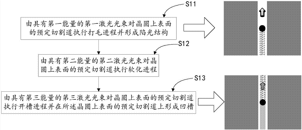
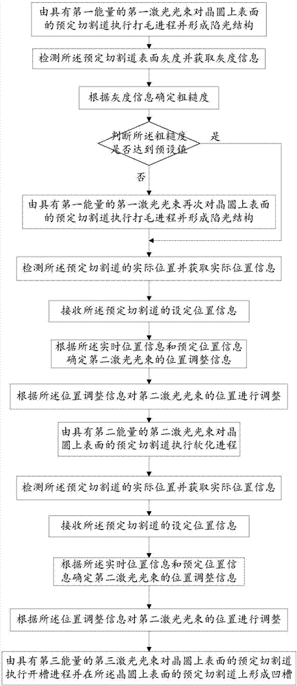
[0057] An embodiment of the present invention provides a method for laser processing a wafer, wherein at least two laser beams with different energy distributions respectively perform a roughening process and a grooving process on a predetermined cutting line on the upper surface of the wafer in sequence, using A groove is formed on the prede...


PUM


Abstract

The invention provides a laser machining method and device for a wafer. The method comprises that at least two laser beams having different energy distribution respectively execute a hacking process and a grooving process on a predetermined cutting path on the upper surface of the wafer in sequence and are used for forming a groove in the predetermined cutting path on the upper surface of the wafer. The predetermined cutting path on the upper surface of the wafer can be hacked by the laser beams with lower energy, the surface of the predetermined cutting path is roughened to improve a light absorptivity, which is convenient for preparation for a subsequent machining process, and the wafer is prevented from being damaged by stripping of a Low-K material caused by a fact that a Low-K layer on the surface of the wafer is machined by adopting the laser beams with over high energy; and meanwhile, the control precision on the energy of the laser beams in a subsequent machining process is higher, and further a laser machining effect of the upper surface of the wafer is improved.

Description

technical field [0001] The invention relates to the technical field of semiconductor processing, in particular to a method and device for laser processing wafers. Background technique [0002] In recent years, with the continuous reduction of the feature size of semiconductor devices and the continuous improvement of chip integration, the parasitic capacitance between metal interconnections and multilayer wiring and the resistance of metal wires have increased sharply, resulting in RC delays, A series of problems such as increased power consumption limit the development of high-speed electronic components. When the feature size of the device is smaller than 90nm, the wafer must use low dielectric constant material instead of traditional SiO 2 Layer (K ​​= 3.9 ~ 4.2), commonly used Low-K materials include Dow Corning's FOx and porous SiLK materials, Applied Materials' black diamond series low-K thin film materials, Novellus System's CORAL, Intel's CDO and NEC's FCN+ organic...

Claims


Application Information

Patent Timeline
Patent Type & Authority Applications(China)
IPC IPC(8): B23K26/364B23K26/36B23K26/70
CPCB23K26/36B23K26/364B23K26/702B23K26/705B23K2101/40
Inventor 侯煜刘嵩张紫辰
Owner 北京中科镭特电子有限公司
Why Eureka
Try Eureka