Flexible conductive film

A flexible conductive and flexible technology, applied in the optical field, can solve the problems of low adhesion, easy falling off of the nano-silver wire layer, cumbersome process, etc., and achieve the effect of improving the performance of blocking water vapor, not easy to break, and simple manufacturing process

Inactive Publication Date: 2017-10-03
ZHANGJIAGANG KANGDE XIN OPTRONICS MATERIAL
View PDF5 Cites 13 Cited by
  • Summary
  • Abstract
  • Description
  • Claims
  • Application Information

AI Technical Summary

Problems solved by technology

[0003] In the prior art, the preparation of nano-silver wire conductive film usually requires repeated steps such as soaking nano-silver wire and hot-pressing process. The process is cumbersome, and after each repeated operation, an optical interface will be formed on the joint surface. Will greatly reduce the light transmittance of the conductive film
Chinese patent document CN102214499 discloses a method for making a transparent conductive film. The steps include: coating a hydrophilic transparent resin on a soft transparent substrate, drying the hydrophilic transparent resin, soaking the dried hydrophilic transparent Resin in the dispersion liquid of nano-silver wire, hot-press the hydrophilic transparent resin, let the nano-silver wire enter the hydrophilic transparent resin, and repeat the soaking and hot-pressing steps several times, the conductive film produced by this method , low light transmittance
[0004] There is another method i

Method used


Image

  • Flexible conductive film
  • Flexible conductive film
  • Flexible conductive film

Examples


Embodiment 1

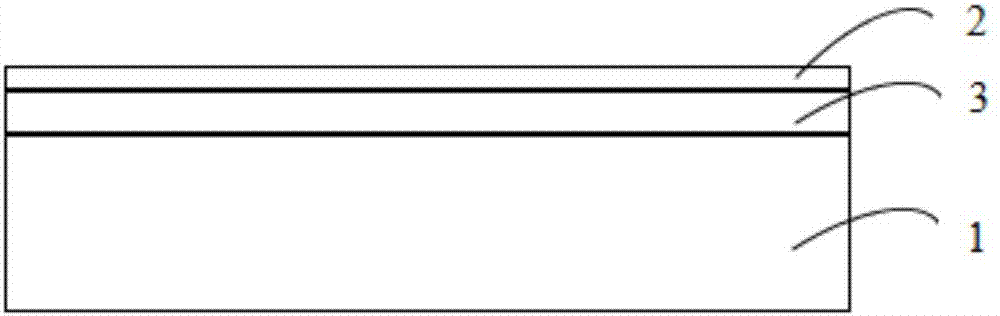
[0043] See figure 1 , a flexible conductive film, including a flexible base material layer 1, a flexible conductive layer 2 and a flexible water vapor barrier layer 3, the flexible water vapor barrier layer 3 is arranged on one side surface of the flexible base material layer 1, and the flexible conductive layer 2 is arranged on the flexible water vapor barrier layer On the surface of layer 3 on the side away from flexible substrate layer 1, the specific preparation steps are as follows:

[0044]S1. Provide a flexible substrate layer 1 as a substrate. The flexible substrate layer 1 can be prepared by a screw extruder, which specifically includes melting the optical film particles required to form the substrate layer, and then extruding with a screw. The machine uniformly extrudes the base material layer material in the molten state to form a film-like flexible base material layer 1, and longitudinally or transversely stretches the formed flexible base material layer 1, so that...

Embodiment 2

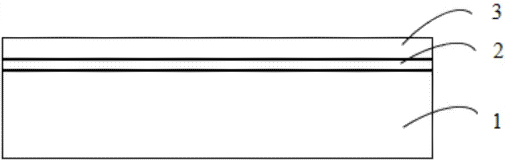
[0050] See figure 2 , a flexible conductive film, including a flexible substrate layer 1, a flexible conductive layer 2 and a flexible water vapor barrier layer 3, the flexible conductive layer 2 is arranged on one side surface of the flexible substrate layer 1, and the flexible water vapor barrier layer 3 is arranged on the flexible conductive layer 2 on the surface of the side away from the flexible substrate layer 1, the specific preparation steps are as follows:

[0051] S1. Provide a flexible substrate layer 1 as a substrate, and the preparation of the flexible substrate layer 1 is the same as that described in Embodiment 1;

[0052] S2. Prepare a flexible conductive layer 2 on the surface of the flexible substrate layer 1. Preferably, the coating solution mixed with silver nanowires is evenly coated on one side surface of the flexible substrate layer 1 to form a flexible conductive layer 2. The coating thickness of the flexible conductive layer is controlled between 5-...

Embodiment 3

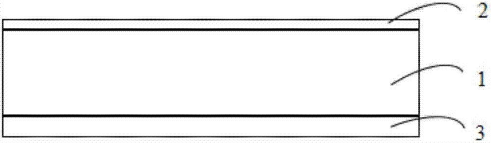
[0056] See image 3 , a flexible conductive film, including a flexible substrate layer 1, a flexible conductive layer 2 and a flexible water vapor barrier layer 3. The difference from Embodiment 1 and Embodiment 2 is that at this time, the flexible substrate layer 1 is located in the middle, and the flexible conductive layer 2 and the flexible water vapor barrier layer 3 are located on both sides of the flexible substrate layer 1 respectively, so that the flexible substrate layer 1 can be better protected from oxidation, corrosion, and the influence of the external environment. The specific preparation steps as follows:

[0057] S1. Provide a flexible substrate layer 1 as a substrate, and the preparation of the flexible substrate layer 1 is the same as that described in Embodiment 1 and Embodiment 2;

[0058] S2. Prepare the flexible conductive layer 2 and the flexible water vapor barrier layer 3 on both sides of the flexible substrate layer 1 respectively. The preparation me...


PUM

PropertyMeasurementUnit
Thicknessaaaaaaaaaa

Abstract

The invention provides a flexible conductive film which comprises a flexible base layer, a flexible conductive layer and a flexible water vapor barrier layer. The flexible base layer, the flexible conductive layer and the flexible water vapor barrier layer are laminated to each other and are combined to form the flexible conductive film. The flexible conductive film is not easy to break, has the advantages of scrape resistance, scratch resistance, bending folding resistance, high light transmittance, low haze, water vapor resistance and the like, can be widely used in a variety of optoelectronic devices, and especially optoelectronic devices with flexible demand and waterproof demand.

Description

technical field [0001] The invention relates to the field of optical technology, in particular to a flexible conductive film. Background technique [0002] Transparent conductive films have the advantages of low resistance and high transmittance. In recent years, they have been widely used in the fields of material science, energy, information, and microelectronics industries. Transparent conductive films have also become the focus of industry research. [0003] In the prior art, the preparation of nano-silver wire conductive film usually requires repeated steps such as soaking nano-silver wire and hot-pressing process. The process is cumbersome, and after each repeated operation, an optical interface will be formed on the joint surface. It will greatly reduce the light transmittance of the conductive film. Chinese patent document CN102214499 discloses a method for making a transparent conductive film. The steps include: coating a hydrophilic transparent resin on a soft tra...

Claims


Application Information

Patent Timeline
IPC IPC(8): H01B5/00H01B5/14B82Y30/00B82Y40/00
CPCH01B5/14B82Y30/00B82Y40/00H01B5/002
Inventor 陈西宝于甄李硕
Owner ZHANGJIAGANG KANGDE XIN OPTRONICS MATERIAL
Why Eureka
Try Eureka