Eureka AIR delivers breakthrough ideas for toughest innovation challenges, trusted by R&D personnel around the world.

Gallium nitride semiconductor device and preparation method thereof

A gallium nitride and semiconductor technology, used in semiconductor devices, semiconductor/solid-state device manufacturing, electrical components, etc., can solve the problems of leakage, breakdown, and device reliability hazards of gallium nitride semiconductor devices

Active Publication Date: 2017-10-13
SHENZHEN JING XIANG TECH CO LTD
View PDF7 Cites 0 Cited by
  • Summary
  • Abstract
  • Description
  • Claims
  • Application Information

AI Technical Summary

Problems solved by technology

[0004] However, in the prior art, due to the high electric field density, the leakage and breakdown of the GaN semiconductor device will be caused, which will damage the GaN semiconductor device and reduce the reliability of the GaN semiconductor device.
Furthermore, after repeated high-voltage tests of GaN power devices, the breakdown voltage of the device will drift. This unstable behavior is related to charge traps, which will cause harm to the reliability of the device and should be suppressed

Method used


Image

  • Gallium nitride semiconductor device and preparation method thereof
  • Gallium nitride semiconductor device and preparation method thereof
  • Gallium nitride semiconductor device and preparation method thereof

Examples


Embodiment Construction

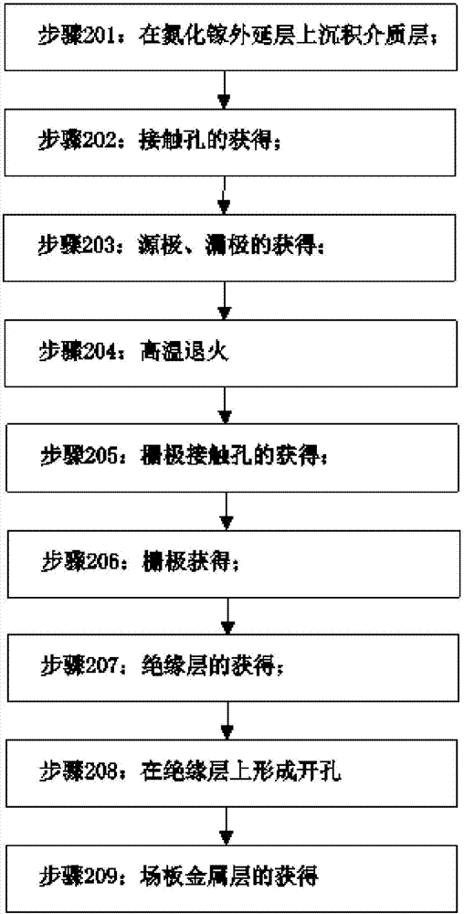
[0029] In order to make the purpose, technical solutions and advantages of the embodiments of the present invention clearer, the technical solutions in the embodiments of the present invention will be clearly and completely described below in conjunction with the drawings in the embodiments of the present invention. Obviously, the described embodiments It is a part of embodiments of the present invention, but not all embodiments. Based on the embodiments of the present invention, all other embodiments obtained by persons of ordinary skill in the art without making creative efforts belong to the protection scope of the present invention.

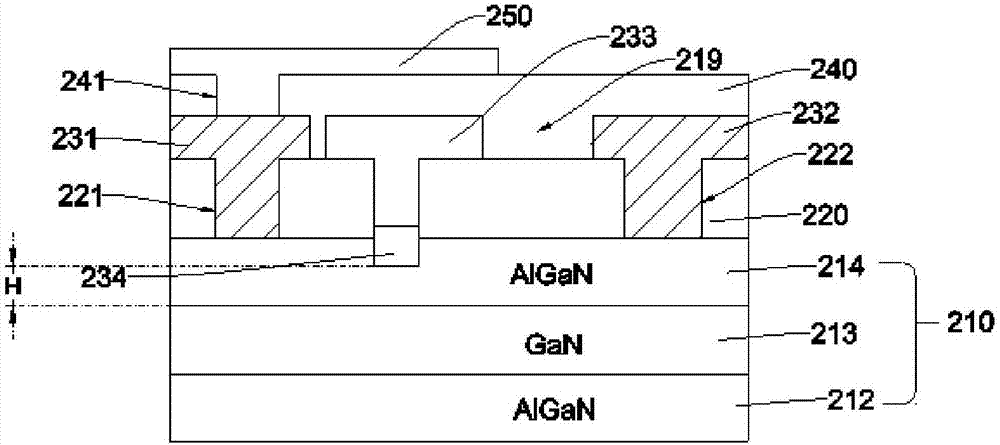
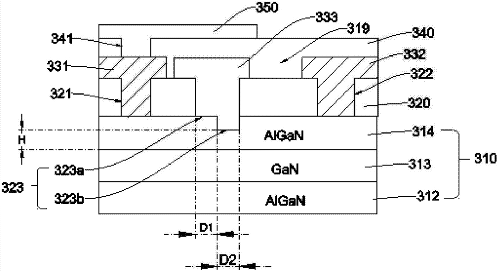
[0030] Such as Figure 1a As shown, the embodiment of the present invention provides a gallium nitride semiconductor device, which includes from bottom to top: gallium nitride epitaxial layer 210, dielectric layer 220, source 231 and drain 232, gate 233, insulating layer 240, field plate metal layer 250 .

[0031] Wherein, the gallium nitrid...


PUM

PropertyMeasurementUnit
thicknessaaaaaaaaaa
thicknessaaaaaaaaaa
thicknessaaaaaaaaaa

Abstract

The invention relates to the technical field of semiconductor materials, and provides a gallium nitride semiconductor device. The gallium nitride semiconductor device comprises a gallium nitride epitaxial layer, a dielectric layer, a source, a drain, a grid and an insulating layer; the dielectric layer is arranged on the gallium nitride epitaxial layer; the source, the drain and the grid are arranged on the dielectric layer; the source, the drain and the grid respectively pass through the dielectric layer, and are connected with the gallium nitride epitaxial layer; the insulating layer is arranged on the source, the drain, the grid and the dielectric layer; and the material of the insulating layer is silicon dioxide. According to the gallium nitride semiconductor device provided by the invention, the phenomenon that an aluminium gallium nitride layer is broken down occurs difficultly; therefore, the electric leakage and breakdown problems of the gallium nitride semiconductor device are avoided; the gallium nitride semiconductor device is effectively protected; and thus, the reliability of the gallium nitride semiconductor device is improved.

Description

technical field [0001] The invention relates to the field of semiconductor technology, in particular to a gallium nitride semiconductor device and a preparation method thereof. Background technique [0002] Gallium nitride has the advantages of large band gap, high electron saturation rate, high breakdown electric field, high thermal conductivity, corrosion resistance and radiation resistance, so gallium nitride can be used to make semiconductor materials to obtain gallium nitride semiconductor devices . [0003] In the prior art, a gallium nitride semiconductor device is prepared by forming a silicon nitride layer on the surface of the gallium nitride epitaxial layer, etching a source contact hole and a drain contact hole on the silicon nitride layer, and Deposit metal in the electrode contact hole and drain contact hole to form the source and drain; then etch the silicon nitride layer and the aluminum gallium nitride layer in the gallium nitride epitaxial layer to form a ...

Claims


Application Information

Patent Timeline
Patent Type & Authority Applications(China)
IPC IPC(8): H01L29/06H01L29/40H01L29/423H01L29/47H01L21/335H01L29/778
CPCH01L29/0611H01L29/0638H01L29/402H01L29/42356H01L29/475H01L29/66462H01L29/7783
Inventor 刘美华林信南刘岩军
Owner SHENZHEN JING XIANG TECH CO LTD
Why Eureka
Eureka Blog
Learn More