OLED display panel and electronic equipment including same

A technology for display panels and electron transport layers, applied in circuits, electrical components, electrical solid devices, etc., can solve the problems of slow material mobility, crosstalk, and poor cleaning effect of evaporation mask, so as to solve difficult cleaning and avoid crosstalk. Effect

Active Publication Date: 2017-10-20
WUHAN TIANMA MICRO ELECTRONICS CO LTD +1
View PDF8 Cites 3 Cited by
  • Summary
  • Abstract
  • Description
  • Claims
  • Application Information

AI Technical Summary

Problems solved by technology

[0004] There are several problems in the existing hole transport material technology. First, the solubility of the material is not good, which will lead to poor cleaning effect of the evaporation mask during mass production.
Second, the mobility of the material is too slow, which can lead to a too high overall voltage of the device
Third, the mobility of the material is too fast, especially the lateral mobility of the material is too fast, resulting in crosstalk between adjacent pixels
[0005] The commercially available material in EP-721935 has an acceptable mobility and no crosstalk, but the solubility is not very good
The commercially available material of CN103108859 is not bad in solubility, but the mobility is too fast, which will cause lateral leakage current and form crosstalk

Method used


Image

  • OLED display panel and electronic equipment including same
  • OLED display panel and electronic equipment including same
  • OLED display panel and electronic equipment including same

Examples


Embodiment 1

[0077]

[0078] Add 5g (13.8mmol) of intermediate 1, 2.3g (6.9mmol) of intermediate 2, 30.9mg (0.138mmol) of palladium acetate and 1.1g (13.9mmol) of sodium tert-butoxide into a 500mL three-necked flask. The flask was replaced with nitrogen, and 100 mL of dehydrated toluene and 0.12 mL (0.276 mmol) of tri-tert-butylphosphine were injected into the flask. Place in an oil bath, slowly heat to 110°C and stir for 8 hours, then let stand overnight. The formed solid was dissolved in dichloromethane, washed with 300 mL of saturated brine, and the organic layer was dried over magnesium sulfate. Recrystallization was carried out using a mixed solvent of toluene and ethanol to obtain 4.3 g (5.0 mmol) of the target compound with a yield of 72%. Mass spectrum M / Z = 900.6 was obtained by LC-MS.

Embodiment 2

[0080]

[0081] Add 5g (14.3mmol) of intermediate 1, 2.3g (6.9mmol) of intermediate 2, 30.9mg (0.138mmol) of palladium acetate and 1.1g (13.9mmol) of sodium tert-butoxide into a 500mL three-necked flask. The flask was replaced with nitrogen, and 100 mL of dehydrated toluene and 0.12 mL (0.276 mmol) of tri-tert-butylphosphine were injected into the flask. Place in an oil bath, slowly heat to 110°C, stir for 8 hours, and let stand overnight. The formed solid was dissolved in dichloromethane, washed with 300 mL of saturated brine, and the organic layer was dried over magnesium sulfate. Recrystallization was carried out using a mixed solvent of toluene and ethanol to obtain 4.5 g (5.17 mmol) of the target compound with a yield of 75%. Mass spectrum M / Z = 876.5 was obtained by LC-MS.

[0082] Example 1

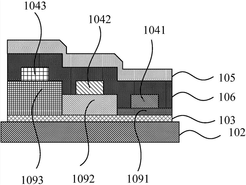
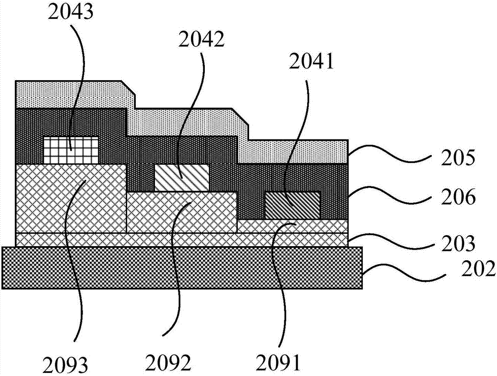
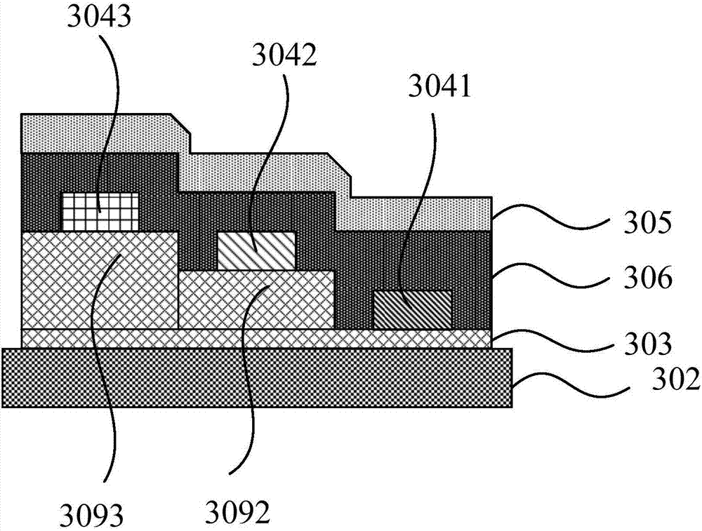
[0083] preparation specific Figure 4 The fabrication process of the OLED display panel with the structure shown is as follows:

[0084] On a glass substrate, form a reflec...

Embodiment 3

[0088] The difference from Example 1 is that the material of the hole transport layer is replaced by Its hole mobility is 2.5×10 -4 cm 2 / V·S, the solubility in NMP is 12g / L.


PUM

PropertyMeasurementUnit
Mobilityaaaaaaaaaa
Solubilityaaaaaaaaaa

Abstract

The present invention relates to an OLED display panel including a first electrode, and a first hole transport layer, a second hole transport layer, an electron transport layer, and a second electrode which are formed in sequence over the first electrode. The second electrode is formed on the electron transport layer. At least two light emitting units are disposed on the second hole transport layer, the electron transport layer covers the light emitting units, and the material of the electron transport layer fills gaps in the adjacent light emitting units, and the first hole transport layer includes a hole transport material having a hole mobility of 9 * 10 <-5> to 5 * 10 <-4> cm 2 / V.S. The hole transport material has a solubility of not less than 10 g / L in N-methylpyrrolidone below 25 DEG C. In the present invention, the hole transporting material with the specific hole mobility is selected as the common hole transport layer, which can avoid crosstalk between different pixels, and can specifically solve the problem that MASK is not easily cleaned due to the specific solubility range of the MASK cleaning solvent.

Description

technical field [0001] The invention belongs to the technical field of organic light-emitting diodes, and in particular relates to an OLED display panel and electronic equipment including the same. Background technique [0002] Many small and medium-sized OLED screens such as mobile phones use R, G, and B sub-pixel display methods (such as figure 1 ). In order to improve the production yield, some functional layers are often designed as common layers, so that FFM (fine metal mask) can be used less, and the hole transport layer often uses a common layer. Generally, the common hole transport layer can be commercially available Material. The molecular structure of commercially available hole transport layer materials is as follows: (EP-721935), but the vertical mobility of this material is relatively high, the lateral mobility is not very high, and there will be no crosstalk between pixels (Cross talk). [0003] CN103108859 discloses The material has better solubility an...

Claims


Application Information

Patent Timeline
IPC IPC(8): H01L27/32H01L51/54H01L51/52H01L51/50
CPCH10K85/111H10K50/11H10K50/16H10K50/156H10K59/35H10K71/166H10K85/636H10K85/626H10K85/631H10K85/342H10K50/155H10K71/00H10K85/633H10K50/15H10K50/852H10K59/30H10K85/615
Inventor 王湘成柳晨何为牛晶华滨田刘营
Owner WUHAN TIANMA MICRO ELECTRONICS CO LTD
Why Eureka
Try Eureka