

Methods to improve chamfer area defects in laser cutting process
A technology of laser cutting and regional defects, which is applied in laser welding equipment, welding/cutting media/materials, manufacturing tools, etc., can solve problems such as chamfering irregular shapes and affecting the performance of OLED display panel products, and achieve heat absorption, Reduce the generation of micro-defects and macro-defects, and improve the effect of micro-crack propagation
- Summary
- Abstract
- Description
- Claims
- Application Information
AI Technical Summary
Problems solved by technology
Method used
Image

Examples
Embodiment Construction
[0028] The specific implementation of the method for improving chamfering area defects in the laser cutting process provided by the present invention will be described in detail below in conjunction with the accompanying drawings.
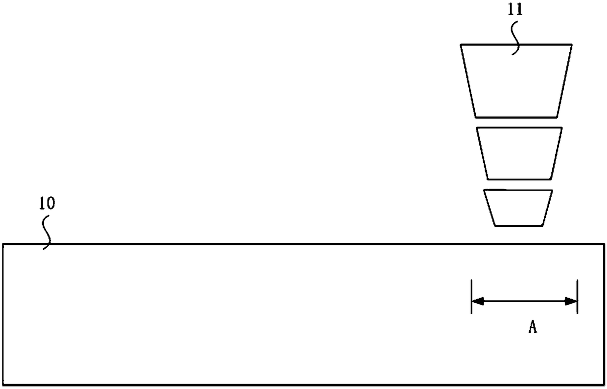
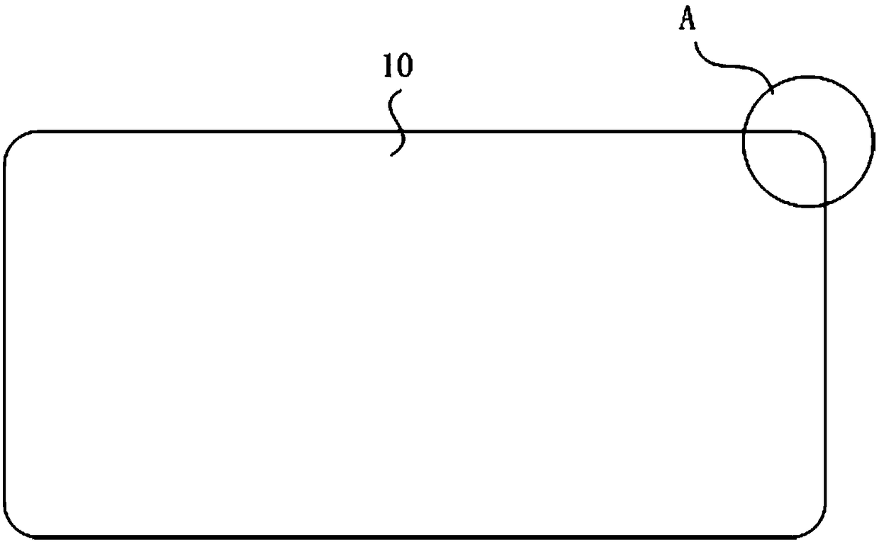
[0029] In the prior art, see Figure 1E , in the area of the chamfered area A, if the laser 11 is directly irradiated on the surface of the display panel in the chamfered area, a heat-affected zone and a crack area will be formed within a certain range, and microscopic defects and macroscopic defects are likely to occur. In view of this, the present invention provides a method for improving defects in the chamfering area in the laser cutting process, which can overcome the above defects and significantly improve the defects in the chamfering area in the laser cutting process.
[0030] figure 2 It is a schematic diagram of the steps of the method for improving the defects in the chamfering area in the laser cutting process of the present inventi...
PUM
 Abstract
Description
Claims
Application Information