Application for taking thin film transistor with adjustable threshold voltage as nonvolatile memory

A thin-film transistor and threshold voltage technology, which is applied in the field of semiconductor non-volatile memory, can solve the problems of small storage window, affecting the working speed of the device, and low erasing efficiency of charge-type NVM, so as to enhance storage performance and improve reliability. Effect

Active Publication Date: 2017-10-27
SOUTHEAST UNIV
View PDF9 Cites 5 Cited by
  • Summary
  • Abstract
  • Description
  • Claims
  • Application Information

AI Technical Summary

Problems solved by technology

In addition, InGaZnO also has the characteristics of being difficult to invert (that is, under negative bias, no holes appear on the surface of InGaZnO), which on the one hand makes TFT have extremely low leakage and reduces TFT power consumption; on the other hand, it also leads to The problems of low erasing efficiency and small storage window of charge-type NVM have become a major bottleneck restricting the development of NVM
In addition, for charge-type NVM, the charges trapped in the storage layer will also scatter the carriers on the surface of the channel layer, which reduces the mobility of the device, thereby affecting the working speed of the device.

Method used


Image

  • Application for taking thin film transistor with adjustable threshold voltage as nonvolatile memory
  • Application for taking thin film transistor with adjustable threshold voltage as nonvolatile memory

Examples


Embodiment Construction

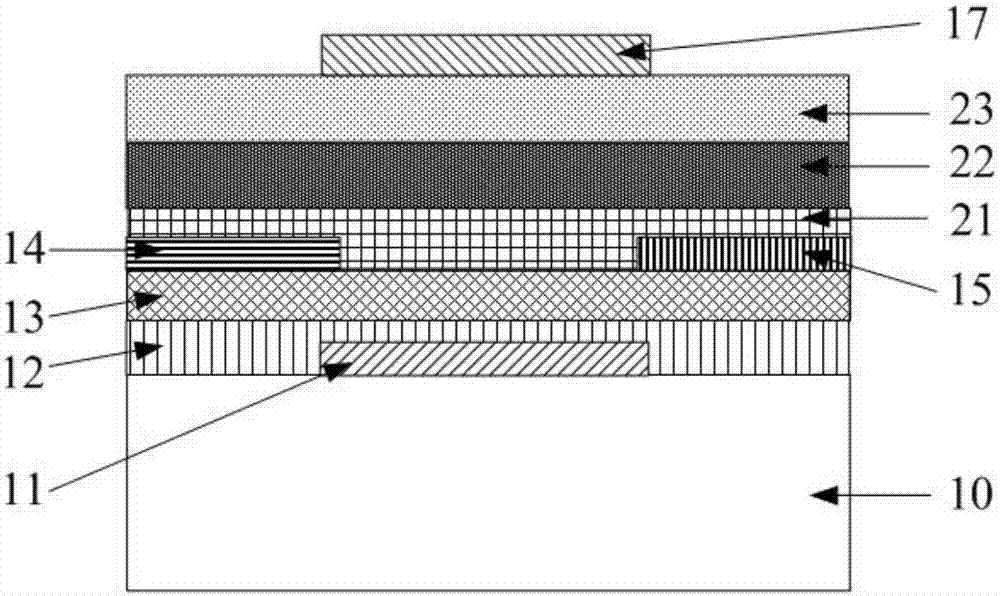
[0015] A thin film transistor with adjustable threshold voltage is used as a non-volatile memory. The thin film transistor with adjustable threshold voltage includes a substrate 10, a bottom gate 11 disposed on the substrate 10, disposed on the substrate 10 and covering The bottom gate oxide layer 12 of the bottom gate 11, the channel layer 13 arranged on the bottom gate oxide layer 12, the source electrode 14 and the drain electrode 15 arranged on opposite sides of the channel layer 13 are arranged on the channel layer 13 and the tunneling layer 21 on the source 14 and the drain 15, the storage layer 22 on the tunneling layer 21, the barrier layer 23 on the storage layer 22, and the top gate 17 on the barrier layer 23, The top gate 17 is located directly above the bottom gate 11 . Wherein, the channel layer 13 is indium gallium zinc oxide, and the equivalent oxide layer thickness T of the bottom gate oxide layer is BOX , The equivalent oxide layer thickness T of the channel ...


PUM


Abstract

The invention discloses an application for taking a thin film transistor with adjustable threshold voltage as a nonvolatile memory. A top-gate memory is formed by the top gate, the barrier layer, the storage layer, the tunneling layer and the channel layer of the thin film transistor; and a bottom-gate TFT (Thin Film Transistor) is formed by the channel layer, the bottom gate oxidization layer and the bottom gate of the thin film transistor. The top-gate memory is operated to realize the ''Program/ Erase'' operation of the nonvolatile memory, and the bottom-gate TFT is operated to realize the ''read'' operation of the nonvolatile memory. Through the separation of the ''Program/ Erase, P/E'' operation and the ''read'' operation, a large memory window of the memory is realized, and the performance, including the reliability, the working speed and the like, of the memory can be improved.

Description

technical field [0001] The invention relates to the field of semiconductor nonvolatile memory, in particular to the use of a thin film transistor as a nonvolatile memory. Background technique [0002] Flat panel displays have been widely used in various electronic products such as TVs, computers, and smart phones, and have greatly improved people's lives. With the rapid increase of people's demand for higher-quality products such as low-power and high-resolution portable electronic devices and large-size 3D displays, researchers have proposed the "System on Panel (SoP)" technology, which puts Modules with different functions (such as pixel circuits, peripheral drive circuits, and information storage modules) are integrated on the panel. SoP technology significantly improves product stability and working speed while reducing product cost and power consumption, so it is a beneficial technical way to develop high-quality flat panel displays. Thin Film Transistor (Thin Film Tr...

Claims


Application Information

Patent Timeline
Patent Type & Authority Applications(China)
IPC IPC(8): G11C19/28H01L29/786
CPCG11C19/28H01L29/786
Inventor 黄晓东黄见秋
Owner SOUTHEAST UNIV
Why Eureka
Try Eureka