Built-in self-test structure of on-chip embedded Flash

A built-in self-test and embedded technology, applied in static memory, instruments, etc., can solve the problems of large hardware overhead, complex test control, large hardware overhead, etc., and achieve the effect of reducing difficulty, simple test control, and avoiding dependence

Active Publication Date: 2017-10-27
XIAN MICROELECTRONICS TECH INST
View PDF5 Cites 3 Cited by
  • Summary
  • Abstract
  • Description
  • Claims
  • Application Information

AI Technical Summary

Problems solved by technology

The hardware overhead of this structure is relatively large, and the execution of test instructions needs to rely on the IEEE1500 structure, and the test control is more complicated; especially for the embedded multi-set FLASH memory, this method requires a relatively large hardware overhead, and the method connects the system through the bus interface module. The connection between the bus and the FBIST controller depends to a certain extent on the functions of the processor and the support of the software, and it still does not get rid of the scope of functional testing.

Method used


Image

  • Built-in self-test structure of on-chip embedded Flash
  • Built-in self-test structure of on-chip embedded Flash
  • Built-in self-test structure of on-chip embedded Flash

Examples


Embodiment

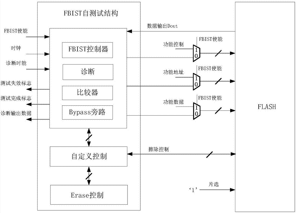
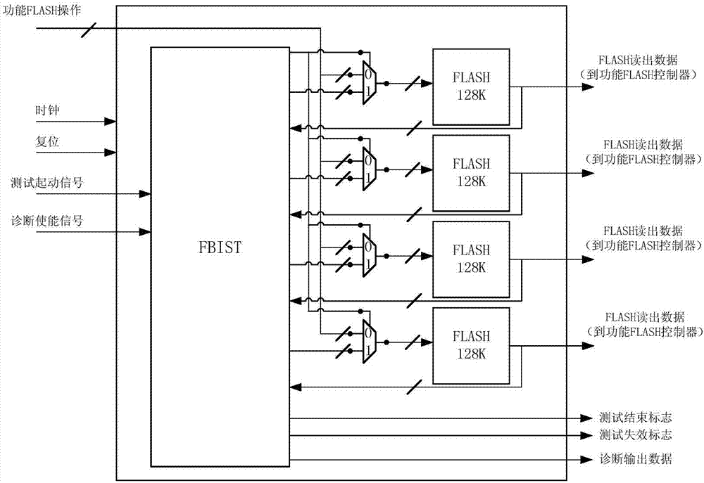
[0033] On a super-large-scale SOC chip with 0.18um process, four pieces of 128K capacity FLASH IP are integrated. This IP supports macro erase and page erase, and the function test access takes a long time and the control is relatively complicated. For the efficient testing of embedded FLASH IP in the circuit, during testability design, the on-chip embedded FLASH built-in self-test structure of the present invention is adopted, and the interface logic is as follows: image 3 shown.

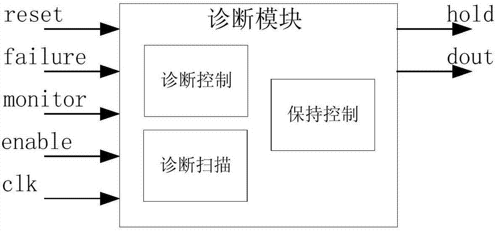
[0034]In the design, considering the scale and test time of FLASH, parallel test technology is adopted. With the support of the built-in self-test structure of the present invention, four 128K FLASHs are tested in parallel, and one FBIST controller performs test control uniformly. When the FBIST circuit is enabled, the controller generates test data, addresses and control signals according to the algorithm sequence under the control of the state machine operation and the custom module, and realize...


PUM


Abstract

The invention provides a built-in self-test structure of an on-chip embedded Flash. The structure comprises a custom control module, an FBIST controller, an ERASE module and a BYPASS module. After being enabled, the FBIST controller initiates operation; according to mutual matching between an internal controller state machine and the custom control module and between the internal controller state machine and the ERASE module, address and reading / writing sequence operation and erasure switching are realized; a readout result and an on-chip comparator are subjected to test result comparison; a result representation signal is output; when a test is ended, a test completion mark jumps; internal access of the FLASH and test result comparison are realized; only a test starting signal and a controller clock signal are required externally; after the test is ended, a test result is represented with a test completion flag bit and a test failure flag bit; a failure address, an algorithm execution state, a reading / writing state and output data information of the FLASH can be mastered, so that a basis is provided for further fault locating; and the built-in self-test of the chip-level or system-level embedded FLASH is realized.

Description

【Technical field】 [0001] The invention belongs to the technical field of testability design of embedded Flash of VLSI such as SoC and DSP, and relates to a built-in self-test structure of on-chip embedded Flash. 【Background technique】 [0002] As the integrated circuit manufacturing process enters the ultra-deep sub-micron stage, the embedded memory occupies an increasing proportion in the SOC system chip. It is predicted that by 2016, the area of ​​the embedded memory on the chip will account for the complex SOC chip More than 95% of the area. [0003] FLASH, as a non-volatile memory based on floating gate technology, has its own unique advantages: non-volatile, can be electrically erased and reprogrammed without special external high voltage, low cost, and high density. It is based on the above characteristics that FLASH is increasingly used in embedded systems. However, as the feature size of semiconductor devices continues to shrink, more and more types of defects exis...

Claims


Application Information

Patent Timeline
Patent Type & Authority Applications(China)
IPC IPC(8): G11C29/12
CPCG11C29/12
Inventor 颜伟沈拉民李俊玲
Owner XIAN MICROELECTRONICS TECH INST
Why Eureka
Try Eureka