Camera module and assembly method thereof

A camera module and assembly method technology, applied in image communication, radiation control devices, televisions, etc., can solve the problems of difficult manufacturing reliability, poor image imaging quality, and reduced yield, and achieve a simple and easy assembly method. , The effect of good gold wire extension performance and improved image quality

Active Publication Date: 2017-10-27
GALAXYCORE SHANGHAI
View PDF7 Cites 15 Cited by
  • Summary
  • Abstract
  • Description
  • Claims
  • Application Information

AI Technical Summary

Problems solved by technology

However, CSP packaging has the following obvious problems: 1. It affects product performance: the absorption, refraction, reflection and scattering of light by thick support glass have a great impact on the performance of image sensors, especially products with small pixel sizes; 2. Reliability issues : The thermal expansion coefficient difference between the components in the package structure and the sealing gas in the cavity have reliability problems in the subsequent SMT process or changes in the product use environment; 3 Large investment scale, large environmental pollution control requirements, and long production cycle , the unit chip cost is high, especially for high-pixel and large-size image sensor products
However, COB packaging has the following obvious problems: 1. Dust control is very difficult, requiring ultra-high clean room levels, and manufacturing maintenance costs are high; 2. Product design is customized, the cycle is long, and the flexibility is not enough; 3. It is not easy to scale production ;
However, the FC package has the following obvious problems: 1. The package has high requirements on the PCB substrate, and has a similar thermal expansion coefficient to Si, and the cost is very high; 2. Manufacturing reliability is very difficult, and the connection between all the bumps and pads of the thermosonic is consistent. Very high performance requirements, bumps and pads are hard-connected, and the ductility is not good; 3. The dust control is difficult, the process environment requirements are high, and the cost is high;
[0010] This method of assembling the camera module has the following disadvantages: For the camera module, it is necessary to use high-precision installation equipment to carry out the precise installation of the above step 3, otherwise it will affect the imaging effect of the camera module, and then assembled The qualified rate of finished products of camera modules is not high; especially for high-pixel camera modules, it is difficult to complete the precise installation of the above step 3 with ordinary installation equipment, so that the imaging effect of high-pixel camera modules is affected. Large impact, the imaging quality of the formed image is poor, especially the imaging quality around the image is obviously bad
[0012] The existing wire bonding method is likely to cause poor structural flexibility after packaging, and the subsequent assembly precision of the camera module is high, and the relative position of the lens and the image sensor chip is difficult to control, which affects the performance of the camera module; The process is long and the packaging efficiency is low, resulting in the image sensor chip being exposed to the air for a long time, requiring multiple inspections and cleanings, reducing the yield rate and increasing the cost of the camera module

Method used


Image

  • Camera module and assembly method thereof
  • Camera module and assembly method thereof
  • Camera module and assembly method thereof

Examples


Embodiment Construction

[0041] In the following detailed description of the preferred embodiment, reference is made to the accompanying drawings which form a part hereof. The accompanying drawings show, by way of example, specific embodiments in which the invention can be practiced. The illustrated embodiments are not intended to be exhaustive of all embodiments in accordance with the invention. It is to be understood that other embodiments may be utilized and structural or logical changes may be made without departing from the scope of the present invention. Accordingly, the following detailed description is not limiting, and the scope of the invention is defined by the appended claims.

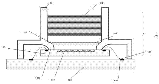
[0042] In order to illustrate the packaging method of the present invention more clearly, in the following embodiments, glass is used as the substrate. Those skilled in the art can understand that the substrate can also be made of other transparent materials.

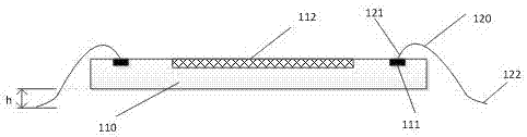
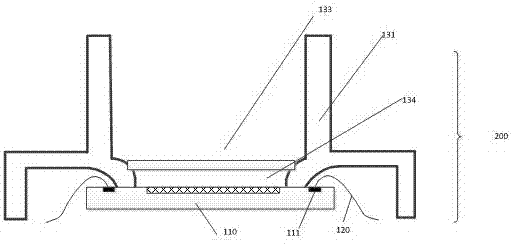
[0043] figure 1 is a schematic diagram of an image...


PUM


Abstract

The invention provides an assembly method for a camera module. The assembly method comprises the following steps: providing an image sensor chip having suspended metal conducting wires, wherein first ends of the metal conducting wires are bonded on welding plates of the image sensor chip, and second ends of the metal conducting wires are suspended away from the image sensor chip; and assembling the image sensor chip, and a supporting frame provided with a light transmitting window into an encapsulation piece, wherein the image sensor chip, the light transmitting window and the supporting frame in the encapsulation piece are formed into a cavity, so that the pollution of external foreign matters to the image sensor chip is reduced; and then, through the second ends of the metal conducting wires, assembling the encapsulation piece with a circuit board and a lens module into the camera module.

Description

technical field [0001] The invention relates to the field of semiconductor manufacturing, in particular to an assembly method of a camera module. Background technique [0002] Currently, mainstream image sensor (CIS: CMOS Image Sensor) packaging methods include: Chip Scale Package (CSP), Chip On Board (COB) and Flip Chip Package (FlipChip, FC) . [0003] CIS CSP is a packaging technology commonly used in low-end, low-pixel (2M pixels or below) image sensors at present, and can adopt Die level (chip level) or Wafer level (wafer level) packaging technology. This packaging technology usually uses wafer-level glass and wafer bonding and uses cofferdams to separate the image sensor chips of the wafer, and then makes pad surface or pad in-plane holes in the pad area of ​​the polished wafer. The through-silicon via technology (TSV: Through Silicon Via) connected by the side ring metal or the T-shaped metal contact chip size packaging technology on the side of the pad after cuttin...

Claims


Application Information

Patent Timeline
Patent Type & Authority Applications(China)
IPC IPC(8): H01L23/488H01L27/146H04M1/02H04N5/225
CPCH01L27/146H01L27/14601H01L27/14683H04M1/0264H01L23/488H04N23/50H01L2924/1815H01L2224/73215
Inventor 赵立新侯欣楠
Owner GALAXYCORE SHANGHAI
Why Eureka
Try Eureka