Laser drilling device and method

A laser drilling and laser technology, which is applied in laser welding equipment, printed circuit, manufacturing tools, etc., can solve the problems of insufficient edge cutting force and residual insulating layer resin materials, etc., to increase speed, avoid pollution, and ensure uniformity Effect

Inactive Publication Date: 2017-11-03
HANS CNC SCI & TECH
View PDF8 Cites 23 Cited by
  • Summary
  • Abstract
  • Description
  • Claims
  • Application Information

AI Technical Summary

Problems solved by technology

[0005] The purpose of the present invention is to solve the existing Gaussian beam drilling method, which has the technical problem that the insulation layer resin material remains on the wall and bottom edge of the PCB microhole due to insufficient edge chipping force.

Method used


Image

  • Laser drilling device and method
  • Laser drilling device and method
  • Laser drilling device and method

Examples


Embodiment Construction

[0032] In order to facilitate the understanding of the present invention, the present invention will be described more fully below with reference to the associated drawings. Preferred embodiments of the invention are shown in the accompanying drawings. However, the present invention can be embodied in many different forms and is not limited to the embodiments described herein. On the contrary, these embodiments are provided to make the understanding of the disclosure of the present invention more thorough and comprehensive.

[0033] Unless otherwise defined, all technical and scientific terms used herein have the same meaning as commonly understood by one of ordinary skill in the technical field of the invention. The terms used herein in the description of the present invention are for the purpose of describing specific embodiments only, and are not intended to limit the present invention.

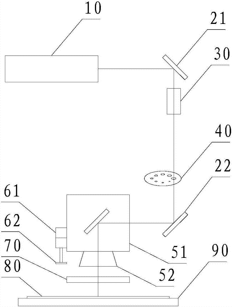
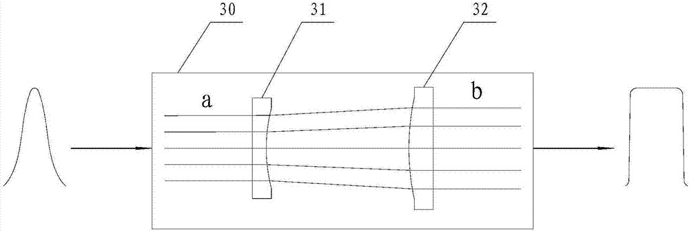
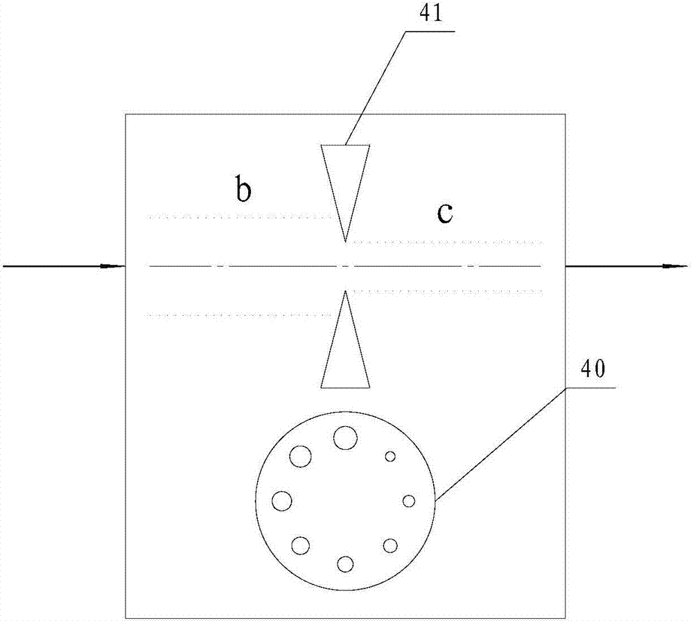
[0034] refer to figure 1 As shown, a laser drilling device includes a laser 10, a f...


PUM


Abstract

The invention provides a laser drilling device and method. The device comprises a laser, a first reflecting mirror, a second reflecting mirror, a beam shaping system, a galvanometer scanning and focusing system, a machined workpiece PCB and a machining platform; The machined workpiece PCB is arranged on the machining platform; the galvanometer scanning and focusing system is located above the machined workpiece PCB; the first reflecting mirror, the beam shaping system and the second reflecting mirror are coaxially arranged from top to bottom and are located at one side of the galvanometer scanning and focusing system; the second reflecting mirror and the galvanometer scanning and focusing system are arranged along the same horizontal axis; and the laser is arranged at one side of the first reflecting mirror along the same horizontal axis. The laser drilling device has the advantages that the influence that residual gum is easily formed due to insufficient cutting force of gauss laser to a drilling edge of the PCB is eliminated by the beam shaping system, and a high-precision and high-quality drilling effect is achieved.

Description

technical field [0001] The invention relates to the field of laser drilling, in particular to a laser drilling device and method. Background technique [0002] Printed circuit board English name: Printedcircuitboard, referred to as PCB board, is based on insulating board, cut to a certain size, and attached with conductive patterns and various functional holes on it, used to replace the substrate of the previous installation of electronic components, And realize the interconnection between electronic components. As the basis for connecting electronic components and drawing electronic conductive graphics, PCB boards have determined their absolute dominance in the electronics industry due to their stable performance, improved automation level, greatly reduced wiring, and improved assembly accuracy. [0003] In the early days, the interconnection between layers of multi-layer PCB boards and the insertion of component pins were all realized by full-through plated through holes....

Claims


Application Information

Patent Timeline
Patent Type & Authority Applications(China)
IPC IPC(8): B23K26/38B23K26/064B23K26/70
CPCB23K26/38B23K26/064B23K26/0648B23K26/702B23K2101/42
Inventor 方志鑫吴超森李强翟学涛杨朝辉高云峰
Owner HANS CNC SCI & TECH
Why Eureka
Try Eureka