Photoconductive switch that reduces on-resistance and preparation method thereof
A technology of photoconductive switch and on-resistance, which is applied in the direction of circuits, electrical components, semiconductor devices, etc., can solve the problems of not paying attention to the energy utilization of devices, etc., to reduce the on-resistance, improve the working life and stability, and enhance the absorption efficiency Effect
- Summary
- Abstract
- Description
- Claims
- Application Information
AI Technical Summary
Problems solved by technology
Method used
Image

Examples
Embodiment 1
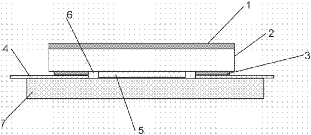
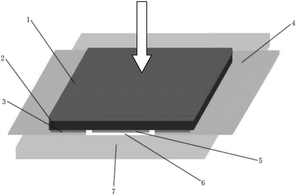
[0047] A photoconductive switch with reduced on-resistance, with a structure such as figure 1 , 2 As shown, it includes a semi-insulating gallium arsenide substrate 2, an anti-reflection film 1 is provided on one side of the substrate 2, electrodes 3 are provided on both sides of the other side, and a high reflection film 5 is provided between the two electrodes.
[0048] The gallium arsenide substrate has a thickness of 600 μm and a dark state resistivity of 5*10 8 Ωcm, electron mobility 4500cm 2 / vs.
[0049] The anti-reflection coating is an optical anti-reflection coating with a reflectivity of less than 0.5% for a wavelength of 1064nm, and the anti-reflection coating is as follows: the first layer is Al with a thickness of 100-200 angstroms 2 o 3 , the second layer is ZrO with a thickness of 1000-1500 Angstroms 2 , the third layer is Al with a thickness of 800-900 angstroms 2 o 3 .
[0050] The high reflection film is a film layer with a reflectivity greater than ...
Embodiment 2
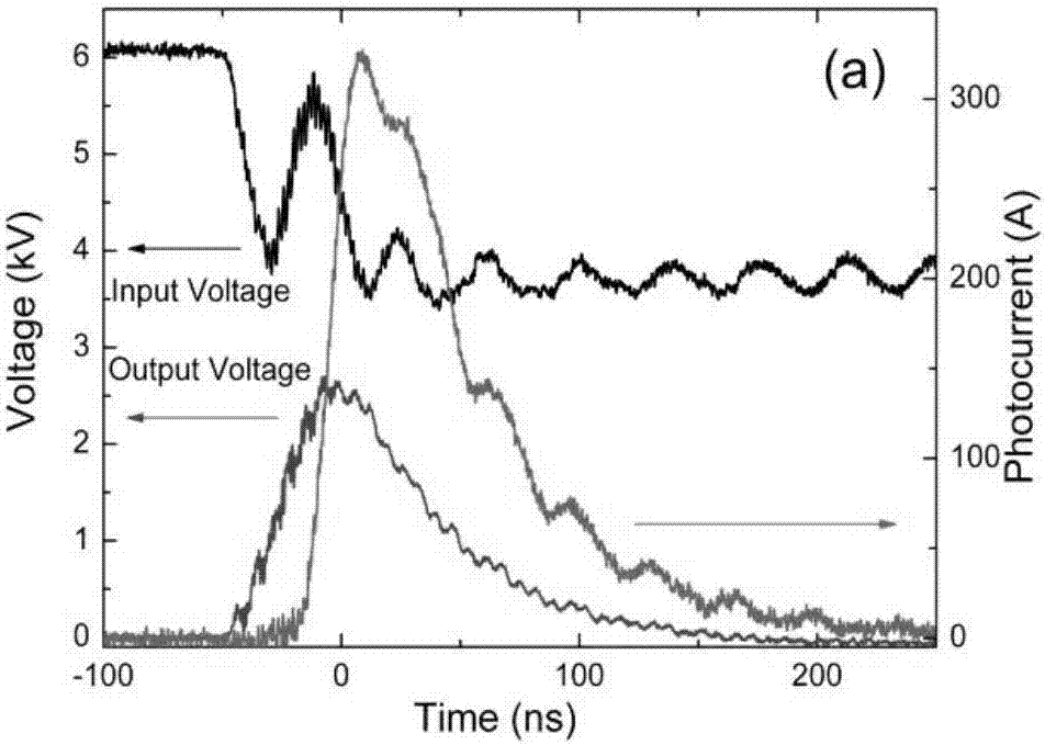
[0063] Example 2: Photoconductive switch on-resistance test experiment
[0064] The test circuit diagram used in the photoconductive switch on-resistance test experiment is as follows: Figure 5 As shown, R is the current limiting resistor 100MΩ, R load is a high-frequency non-inductive resistor 50Ω, C is an energy storage capacitor 1nF, and PCSS represents a photoconductive switch. Test the voltage value through the high-voltage probe, and test the current value through the current loop.
[0065] The structure made in embodiment 2 is tested on the photoconductive switch described in embodiment 1, and the waveform curves of the input voltage, output voltage and load current of the obtained results are as follows Figure 4 shown.
[0066] The gallium arsenide photoconductive switch with no evaporated anti-reflection film and high reflection film whose other structures are the same as in Example 1 was tested, and the waveform curves of the input voltage, output voltage and lo...
PUM
| Property | Measurement | Unit |
|---|---|---|
| Thickness | aaaaa | aaaaa |
| Electron mobility | aaaaa | aaaaa |
| Thickness | aaaaa | aaaaa |
Abstract
Description
Claims
Application Information
PatSnap Eureka turns technology decisions into work you can execute. Powered by our Innovation Knowledge Graph, it runs expert workflows across engineering, life sciences, materials and intellectual property. Get your review-ready output in minutes.


