Surface phasmon coaxial optical waveguide structure

A surface plasmon and waveguide structure technology, applied in the field of optical waveguides, to reduce noise optical signals, increase propagation distance, and reduce losses

Inactive Publication Date: 2009-02-11
XIAMEN UNIV
View PDF2 Cites 7 Cited by
  • Summary
  • Abstract
  • Description
  • Claims
  • Application Information

AI Technical Summary

Problems solved by technology

In recent years, the optical waveguide behavior of semiconductor nanostructures has received extensive attention, but energy loss in information transmission is still unavoidable

Method used


Image

  • Surface phasmon coaxial optical waveguide structure
  • Surface phasmon coaxial optical waveguide structure
  • Surface phasmon coaxial optical waveguide structure

Examples


Embodiment 1

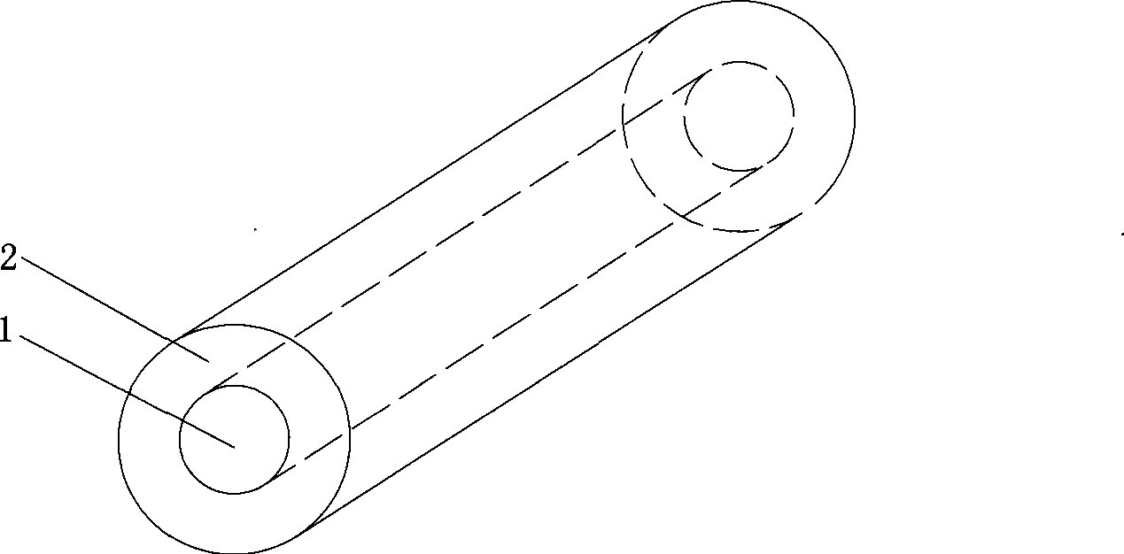
[0019] Surface plasmon coaxial waveguide structure such as figure 1 shown. The structure consists of a cylindrical metal core 1 and a tubular wide bandgap dielectric shell 2 . Wherein the core layer 1 adopts metal zinc, and the dielectric shell layer 2 adopts wide band gap zinc silicate. The diameter of the cylindrical metal core layer is 50nm, and the thickness of the tubular wide-bandgap dielectric shell layer is 25nm, which is less than the half-wavelength of the light wave with a propagation wavelength of 300nm. The structure can be prepared by using a quartz tube as a reaction chamber, using flowing nitrogen as a protective gas, and metal zinc powder as a raw material, and reacting and forming on a single crystal silicon substrate. Experimental measurement results show that the resonant cavity provided by surface plasmons in this embodiment has a small mode volume, and its fineness is 10 times and 33 times higher than that of the whispering gallery mode and waveguide mo...

Embodiment 2

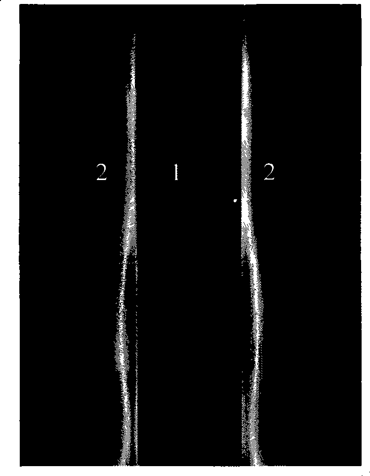
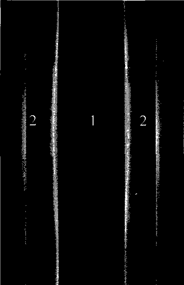
[0021] Similar to Example 1, the difference is that silicon dioxide is used as the shell dielectric material to obtain different target wavelengths. The target wavelength corresponding to this structure is 348nm. For the simulated electromagnetic field distribution, see image 3 , the light energy gain is more than 5 times. It can be seen that by changing the types of core metal material and shell wide bandgap dielectric material, surface plasmon coaxial optical waveguide structures with different target wavelengths can be designed.

Embodiment 3

[0023] Similar to Embodiment 1, the difference is that a gold core layer is used, the diameter of the gold core layer is 10 nm, and the dielectric material of the shell layer is a zinc oxide shell layer.


PUM


Abstract

The invention discloses a surface plasmon coaxial optical wave guide structure which relates to an optical wave guide. The surface plasmon coaxial optical wave guide structure is good for the light signal transmission. A cylindrical core layer and a tubular shell layer are arranged; the cylindrical core layer is a metal core layer; and the shell layer is a wide band-gap media shell layer. The surface plasmon coaxial optical wave guide structure taking metal as the core layer enlarges the transmitted light signal in the wave guide, and provides a resonant cavity with small mode volume, thereby improving fineness and facilitating transmission efficiency of the objective light signal.

Description

technical field [0001] The invention relates to an optical waveguide, in particular to a surface plasmon coaxial optical waveguide structure. Background technique [0002] Since the one-dimensional nanostructure has a size smaller than the wavelength of visible light in the radial direction, the signal light can be effectively transmitted along the axial direction of the nanostructure, which has the function of a waveguide device and can be used to effectively connect various nanophotonic devices or units to implement integrated systems. Various complex tasks. Compared with conventional waveguide devices, semiconductor nano-optical waveguides can emit fluorescence, which can reduce the energy loss caused by optical coupling. In recent years, the optical waveguide behavior of semiconductor nanostructures has received extensive attention, but energy loss in information transmission is still unavoidable. Therefore, how to achieve the local amplification of optical signals in ...

Claims


Application Information

Patent Timeline
Patent Type & Authority Applications(China)
IPC IPC(8): G02B6/02
Inventor 康俊勇庄庆瑞冯夏
Owner XIAMEN UNIV
Why Eureka
Try Eureka