Epitaxial structure of light emitting diode

A technology of light-emitting diodes and epitaxial structures, applied in electrical components, circuits, semiconductor devices, etc., can solve problems such as the inability to effectively increase hole concentration, and achieve the effects of improving internal quantum efficiency, blocking electron overflow, and increasing concentration.

Active Publication Date: 2017-11-21
HC SEMITEK SUZHOU
View PDF5 Cites 0 Cited by
  • Summary
  • Abstract
  • Description
  • Claims
  • Application Information

AI Technical Summary

Problems solved by technology

[0005] Since Mg is used as the acceptor impurity of the P-type layer when injecting holes, the injected hole concentration will be limited by the solid solubility of the acceptor impurity and the high acceptor activation energy, so the hole concentration cannot be effectively increased.

Method used


Image

  • Epitaxial structure of light emitting diode
  • Epitaxial structure of light emitting diode
  • Epitaxial structure of light emitting diode

Examples


Embodiment Construction

[0027] The specific implementation manners of the present invention will be further described in detail below in conjunction with the accompanying drawings and embodiments. The following examples are used to illustrate the present invention, but are not intended to limit the scope of the present invention.

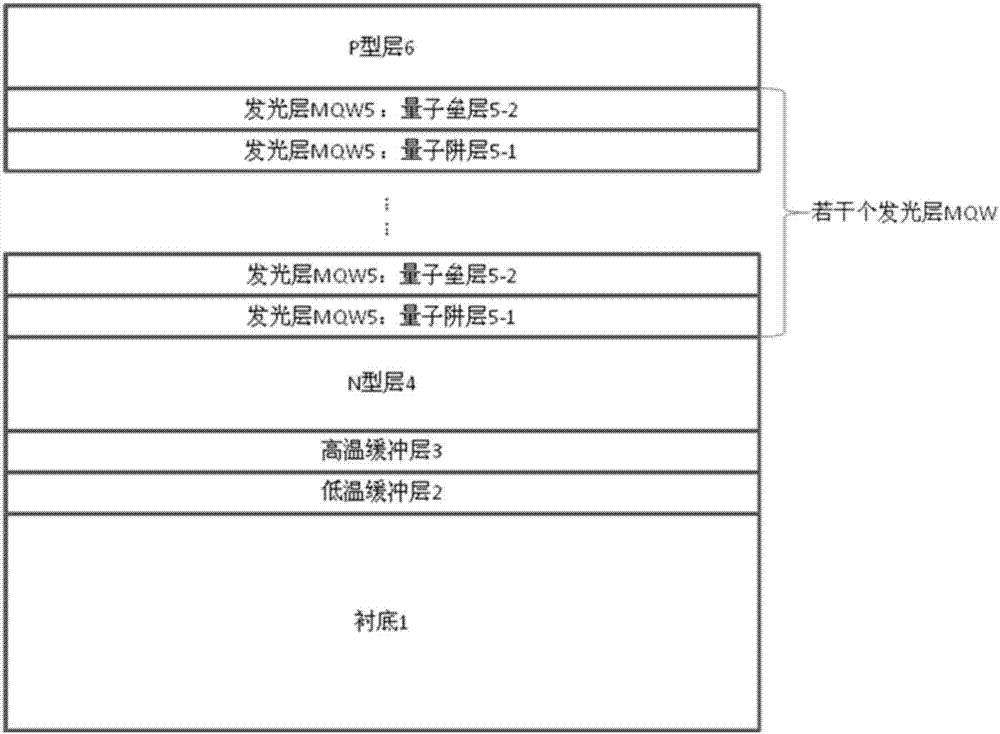
[0028] LED is a semiconductor solid-state light-emitting device, which mainly uses semiconductor P-N junction as a light-emitting structure. In recent years, semiconductor light-emitting diodes represented by gallium nitride have received extensive attention and vigorous research due to their excellent characteristics such as large band gap, high electron saturation electron drift velocity, high temperature resistance, and high power capacity. Breakthrough progress has been made in recent years. At the same time, as a ternary alloy of gallium nitride, indium gallium nitride, its bandgap is continuously adjustable from 0.7ev to 3.4ev, and its luminous wavelength covers the...


PUM


Abstract

The invention provides an epitaxial structure of a light emitting diode, and belongs to the technical field of semiconductor device epitaxy. The epitaxial structure includes an N type layer, a light emitting layer and a P type layer; the light emitting layer is located between the N type layer and the P type layer and covers the N type layer, and the P type layer covers the light emitting layer; and a direction from the light emitting layer to the P type layer is the growth direction of the potential barrier of the P type layer, and the potential barrier of the P type layer gradually decreases along the growth direction. The potential barrier of the P type layer decreases progressively along the epitaxial growth direction, so that the potential barrier in the direction from the P type layer to the light emitting layer gradually increases, thereby facilitating entering of more holes into the light emitting layer, reducing a blocking effect on holes, and thus effectively improving the concentration of the holes in the light emitting layer. In addition, the potential barrier of the P type layer gradually decreases along the epitaxial growth direction, so that the potential barrier close to the light emitting layer is the highest, thus electron overflow can be effectively blocked, and the internal quantum efficiency of the light emitting diode can be improved.

Description

technical field [0001] The present invention relates to the technical field of semiconductor device epitaxy, and more specifically, to an epitaxy structure of a light emitting diode. Background technique [0002] LED (Light Emitting Diode, Light Emitting Diode) is a semiconductor solid-state light-emitting device, which mainly uses a semiconductor P-N junction as a light-emitting structure. In recent years, semiconductor light-emitting diodes represented by gallium nitride have received extensive attention and vigorous research due to their excellent characteristics such as large band gap, high electron saturation electron drift velocity, high temperature resistance, and high power capacity. Breakthrough progress has been made in recent years. At the same time, as a ternary alloy of gallium nitride, indium gallium nitride, its bandgap is continuously adjustable from 0.7ev to 3.4ev, and its luminous wavelength covers the entire region of visible light and ultraviolet light, ...

Claims


Application Information

Patent Timeline
Patent Type & Authority Applications(China)
IPC IPC(8): H01L33/06H01L33/12H01L33/32
CPCH01L33/06H01L33/12H01L33/325
Inventor 刘华容胡加辉万林
Owner HC SEMITEK SUZHOU
Why Eureka
Try Eureka