Strain loading system for micro-nano material multi-field joint characterization

A technology of micro-nano materials and loading systems, which is applied in the fields of analysis materials, measuring devices, instruments, etc., can solve the problems that cannot meet the requirements of micro-nano material elastic strain engineering research, the difficulty of testing the electrical properties of target materials, and the difficulty of applying strain with low precision, etc. problem, to achieve the effect of simple structure, improved universality and reliable performance

Active Publication Date: 2017-12-01
咸阳瞪羚谷新材料科技有限公司
View PDF6 Cites 4 Cited by
  • Summary
  • Abstract
  • Description
  • Claims
  • Application Information

AI Technical Summary

Problems solved by technology

But the disadvantages are: 1. The applied strain has been fixed and cannot be changed; 2. In the process of material growth, the dislocation of the substrate will inevitably be introduced into the studied material, resulting in the maximum strain that the target material can bear is limited. Great limitations; 3. This method cannot apply strain to chemically grown one-dimensional or two-dimensional materials; 4. It is difficult to test the electrical properties of target materials
The flexible substrate deformation method uses a flexible substrate instead of the above-mentioned rigid substrate, and the strain range is greatly increased, but the strain state of this method is relatively complicated and the accuracy of the applied strain is low and it is difficult to accurately quantify (Flexible piezoresistive strain sensor based on single Sb-doped ZnOnanobelt, Y.Yang , et al., Applied Physics Letters, 97, 223107, 2010)
[0007] None of the above methods can test and characterize the electrical, optical, and structural properties of micro-nano materials while applying adjustable uniaxial strain to micro-nano materials in a wide range. Strain Engineering Research Requirements

Method used


Image

  • Strain loading system for micro-nano material multi-field joint characterization
  • Strain loading system for micro-nano material multi-field joint characterization
  • Strain loading system for micro-nano material multi-field joint characterization

Examples


Embodiment Construction

[0028] Below in conjunction with accompanying drawing, the present invention is described in further detail:

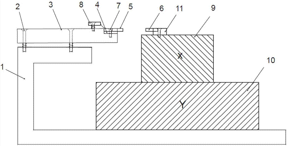
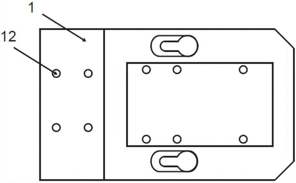
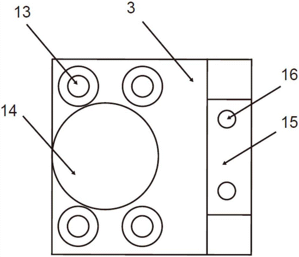
[0029] refer to figure 1 , 2 , a strain loading system for multi-field joint characterization of micro-nano materials according to the present invention includes a substrate 1, a sample stage 3, an electrode pressing piece 8, a metal support 7, a loading stage 5, an indenter 6, and a piezoelectric ceramic 8 And piezoelectric ceramic 9, spring screw 2, set screw 4. The sample stage 3 is fixed on the uppermost end of the base body 1 by the spring screw 2 through the counterbore 13, and the height of the sample stage 3 can be adjusted by adjusting the screwing depth of the spring screw 2. The sample stage 3 has a level 14, which can observe whether the sample stage 3 is whole Keep, ensure that the sample stage 3 remains horizontal after adjusting the depth of the screw, the piezoelectric ceramic 9 and the piezoelectric ceramic 10 are fixed to each other, the piezoelect...


PUM

PropertyMeasurementUnit
lengthaaaaaaaaaa

Abstract

The invention discloses a strain loading system for micro-nano material multi-field joint characterization. A sample stage is fixed to the top end of a base body by spring screws, wherein piezoelectric ceramic is fixed to the upper end of the bottom of the base body, a loading stage is stuck in a metal support groove, a metal support is fixed to a groove in the right side of the sample stage by metal support screws, an electrode pressing sheet is fixed to the upper end of the sample stage, the electrode pressing sheet is in close contact with an electrode on the loading stage to form good electrical contact, a pressure head is fixed in the metal support groove, and the metal support is fixed in the top surface of the piezoelectric ceramic. Strain loading on micro-nano materials in multiple characterization devices is realized; an electrical measurement system has the characteristics of simple structure, reliable performance, simple and convenient installation, convenient operation and wide application scope, can be applied to all one-dimensional or two-dimensional nanomaterials with the length greater than 5 microns, and can be used together with instruments such as various optical microscopes, electron microscopes, spectrometers and synchronous radiometers for multi-field coupling testing.

Description

technical field [0001] The present invention relates to the field of elastic strain research of micro-nano materials, and relates to a method and device for uniaxial strain generation applied to the joint characterization of micro-nano materials with multiple fields (force, electricity, heat, light, etc.), and specifically relates to a microelectronic-based Strain loading system for multi-field characterization of micro-nano materials in mechanical system (MEMS) technology and machining technology. Background technique [0002] John J. Gilman, a world-renowned scholar in the field of material mechanics, explained the theoretical strength of materials (under this stress, the bonds between atoms will be Spontaneous breaking or switching) and drastic electronic structure changes (such as the closing of the semiconductor band gap). Because almost all physical and chemical properties of materials depend on the electronic structure, and the electronic structure must undergo drast...

Claims


Application Information

Patent Timeline
Patent Type & Authority Applications(China)
IPC IPC(8): G01N33/00
Inventor 单智伟王晓光陈凯沈昊张永强
Owner 咸阳瞪羚谷新材料科技有限公司
Why Eureka
Try Eureka