Manufacturing method of semiconductor device

A manufacturing method and semiconductor technology, applied in the direction of semiconductor devices, electrical solid devices, electrical components, etc., can solve problems such as silicon oxide etching damage, affecting device performance and yield, so as to avoid residual problems, improve yield and performance, and avoid Effect of etch damage

Active Publication Date: 2017-12-01
SEMICON MFG INT (SHANGHAI) CORP +1
View PDF3 Cites 7 Cited by
  • Summary
  • Abstract
  • Description
  • Claims
  • Application Information

AI Technical Summary

Problems solved by technology

[0005] However, in the manufacturing process of conventional deep trench capacitors, the process of silicon oxide etching is often included. During the process of silicon oxide etching, it is easy to cause damage to the silicon oxide filled in the shallow trench isolation structure outside the deep trench capacitors. Etch damage, which affects device performance and yield

Method used


Image

  • Manufacturing method of semiconductor device
  • Manufacturing method of semiconductor device
  • Manufacturing method of semiconductor device

Examples


Embodiment Construction

[0034] In the following description, a lot of specific details are given in order to provide a more thorough understanding of the present invention. However, it is obvious to those skilled in the art that the present invention can be implemented without one or more of these details. In other examples, in order to avoid confusion with the present invention, some technical features known in the art are not described.

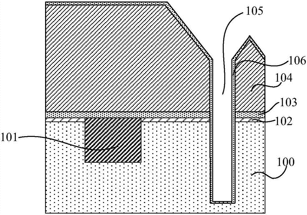
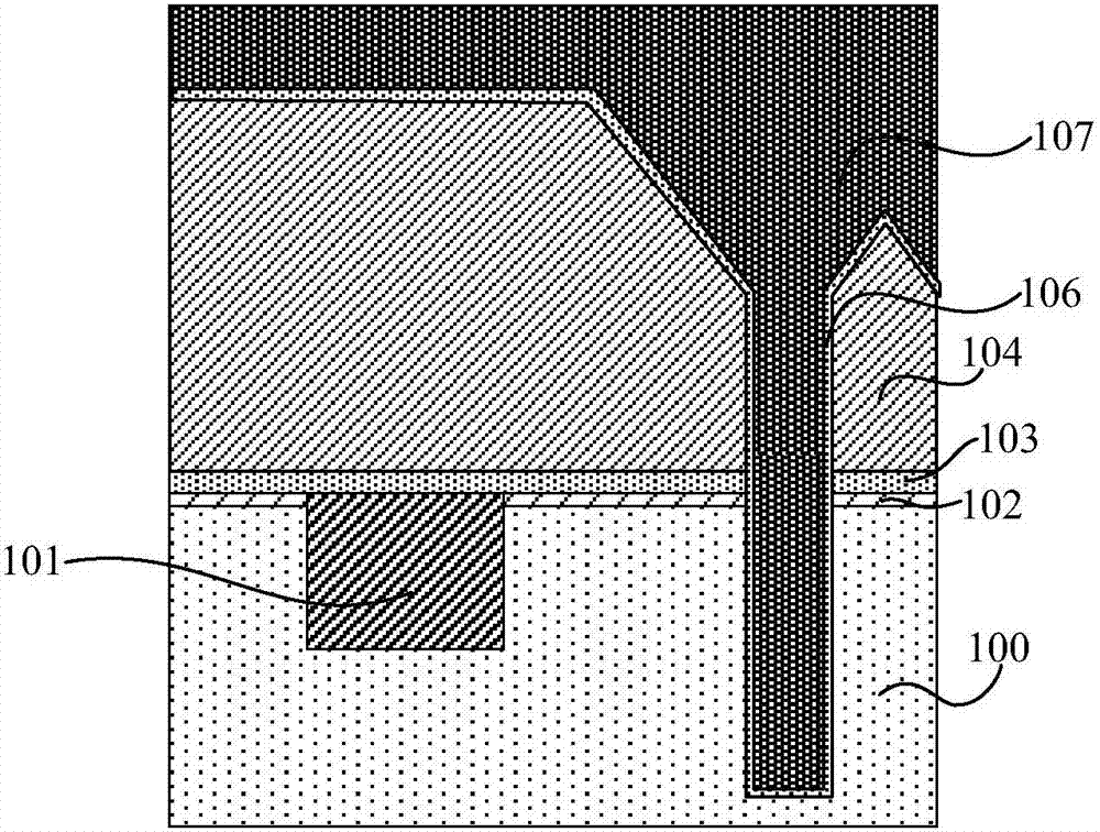
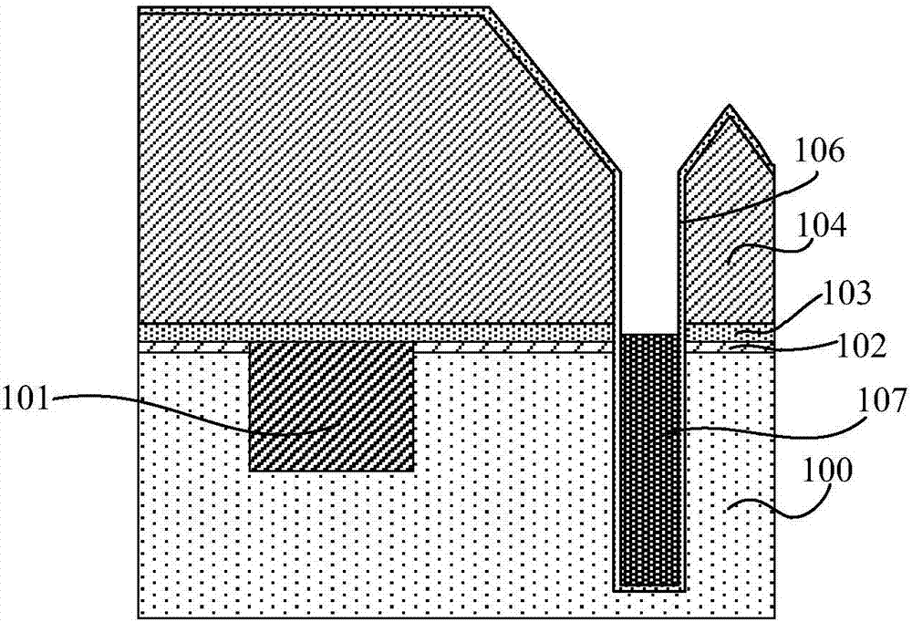
[0035] It should be understood that the present invention can be implemented in different forms and should not be construed as being limited to the embodiments presented here. On the contrary, the provision of these embodiments will make the disclosure thorough and complete, and will fully convey the scope of the present invention to those skilled in the art. In the drawings, the sizes and relative sizes of layers and regions may be exaggerated for clarity. The same reference numerals denote the same elements throughout.

[0036] It should be understood that when an...


PUM


Abstract

The invention provides a manufacturing method of a semiconductor device, and relates to the technical field of semiconductors. The method comprises the steps that a semiconductor substrate is provided, a first dielectric layer is formed on the surface of the semiconductor substrate, and a patterned mask layer is formed on the first dielectric layer; a deep trench arranged in the semiconductor substrate is formed; a second dielectric layer is formed on the bottom part and the side wall of the deep trench; a first polysilicon layer is formed through deposition to fill in the deep trench; the first time of etching is performed to etch and remove partial first polysilicon layer, wherein the top surface of the remaining first polysilicon layer is higher than the top surface of the first dielectric layer and lower than the top surface of the mask layer; the mask layer is removed; the second time of etching is performed to etch and remove the first polysilicon layer; and the top polar plate of the deep trench capacitor is formed. According to the method, etching damage to other film layers or materials which are arranged at the external side of the deep trench and have the same material with that of the mask layer in the removing process of the mask layer can be effectively avoided and the window of the mask layer removing process can be expanded.

Description

Technical field [0001] The present invention relates to the field of semiconductor technology, in particular to a method for manufacturing a semiconductor device. Background technique [0002] In the field of semiconductor technology, an image sensor is a semiconductor device that can convert optical images into electrical signals. Image sensors can be roughly divided into charge coupled devices (CCD) and complementary metal oxide semiconductor image sensors (CMOS Image Sensor, referred to as CIS). The advantages of the CCD image sensor are high image sensitivity and low noise, but it is difficult to integrate the CCD image sensor with other devices, and the power consumption of the CCD image sensor is relatively high. In contrast, CMOS image sensors are gradually replacing CCDs due to their simple process, easy integration with other devices, small size, light weight, low power consumption, and low cost. At present, CMOS image sensors are widely used in the fields of digital c...

Claims


Application Information

Patent Timeline
Patent Type & Authority Applications(China)
IPC IPC(8): H01L27/146
CPCH01L27/14601H01L27/14683H01L27/14687
Inventor 唐文涛王冲包德君王明军
Owner SEMICON MFG INT (SHANGHAI) CORP
Why Eureka
Try Eureka