
Power semiconductor device and manufacturing method thereof

A technology of power semiconductors and devices, which is applied in the field of power semiconductor devices and their production, and can solve problems such as controlling base reverse bias turn-off

Pending Publication Date: 2017-12-08
GLOBAL ENERGY INTERCONNECTION RES INST CO LTD
View PDF5 Cites 4 Cited by
  • Summary
  • Abstract
  • Description
  • Claims
  • Application Information

AI Technical Summary

Problems solved by technology

[0004] In view of this, the embodiment of the present invention provides a power semiconductor device and its manufacturing method to solve the problem that the existing three-terminal power semiconductor cannot be turned off by controlling the reverse bias of the base once it is turned on

Method used


Image

  • Power semiconductor device and manufacturing method thereof
  • Power semiconductor device and manufacturing method thereof
  • Power semiconductor device and manufacturing method thereof

Examples


Embodiment 1

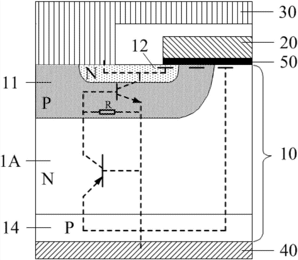
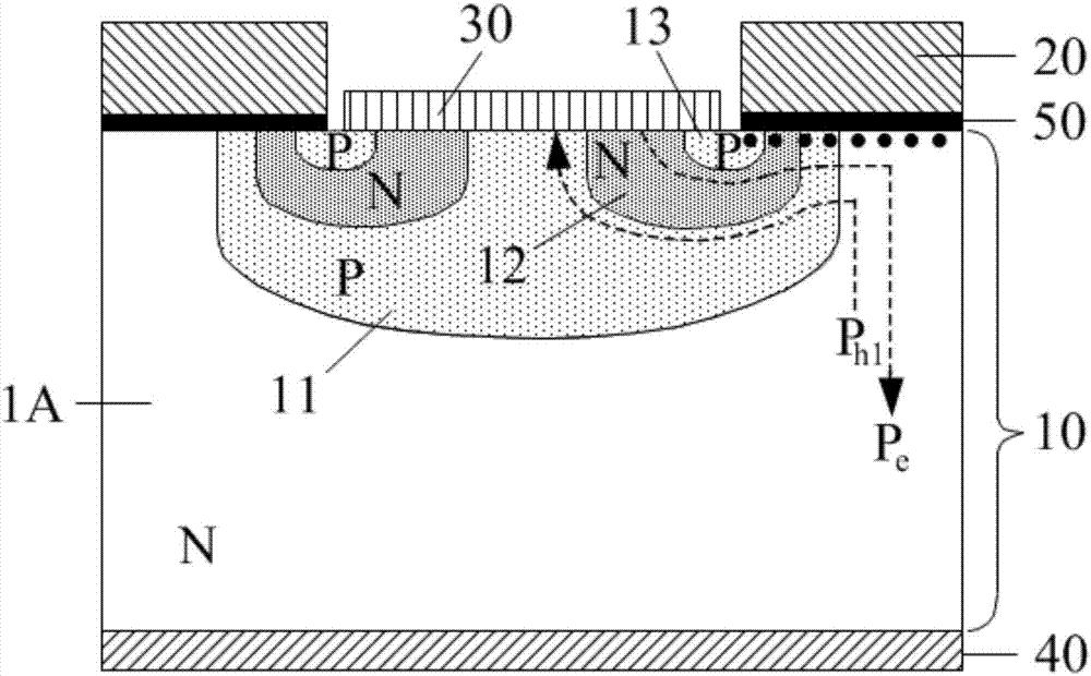
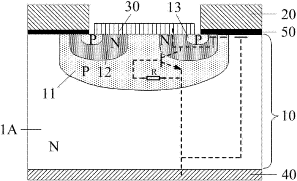
[0028] An embodiment of the present invention provides a power semiconductor device, such as Figure 2 to Figure 4 As shown, the power semiconductor device includes a substrate 10, a first doped layer 11, a second doped layer 12, a third doped layer 13, a control electrode 20, a first electrode 30 and a second electrode 40, wherein the control electrode 20 may be, for example, a gate or a base, the first electrode 30 may be, for example, a source or a collector, and the second electrode may be, for example, a drain or an emitter.

[0029] The substrate 10 has a first surface and a second surface opposite to the first surface, and the substrate 10 is of the first conductivity type, Figure 2 to Figure 4 1A is the original doping type layer of the substrate 10 , that is, the first conductivity type. The first doped layer 11 is disposed in the substrate 10 and is of a second conductivity type opposite to the first conductivity type. The second doped layer 12 is disposed in the ...

Embodiment 2

[0042] An embodiment of the present invention provides a power semiconductor device, such as Figure 5 to Figure 7 As shown, the power semiconductor device includes a substrate 10, a first doped layer 11, a second doped layer 12, a third doped layer 13, a control electrode 20, a first electrode 30, and a second electrode 40. For details, please refer to Implementation example one. The difference between the embodiment of the present invention and the first embodiment is that the fourth doped layer 14 is further included. The fourth doped layer 14 is disposed between the substrate 10 and the second electrode 40 , and the fourth doped layer 14 is of the second conductivity type.

[0043] The working principle of the above-mentioned power semiconductor device will be described below with the first conductivity type being N-type and the second conductivity type being P-type.

[0044] When the control electrode 20 is connected to a positive voltage, such as Figure 5 As shown, m...

Embodiment 3

[0054] An embodiment of the present invention provides a method for manufacturing a power semiconductor device, which is used to manufacture the power semiconductor device described in Embodiment 1, such as Figure 8 As shown, this step includes the following steps:

[0055] S101: Form a first doped layer in a first surface of a substrate of a first conductivity type, where the first doped layer is of a second conductivity type opposite to the first conductivity type.

[0056]S102: Form a second doped layer of the first conductivity type in the first doped layer.

[0057] S103: forming a third doped layer of the second conductivity type in the second doped layer.

[0058] S104: forming an isolation layer on the first surface of the substrate, the isolation layer is in contact with surfaces of the first doped layer, the second doped layer, and the third doped layer.

[0059] S105: forming a control electrode on the isolation layer.

[0060] S106: forming a first electrode on...


PUM


Abstract

The present invention discloses a power semiconductor device and a manufacturing method thereof. The power semiconductor device comprises: a first conductive-type substrate; a first doping layer arranged in the substrate and having a second conductive type being opposite to the first conductive type; a second doping layer arranged in the first doping layer and having the first conductive type; a third doping layer arranged in the second doping layer and having the second conductive type; a control electrode arranged on the first surface of the substrate through an isolation layer, wherein the isolation layer is in contact with the surfaces of the first doping layer, the second doping layer and the third doping layer; a first electrode arranged on the first surface of the substrate, wherein the first electrode is in contact with the surfaces of the first doping layer, the second doping layer and the third doping layer; and a second electrode arranged on the second surface of the substrate. When the control electrode is connected with negative electricity, the third doping layer forms the extraction path of holes of an n-type doping layer so as to reduce the local concentration of carriers and reduce the barrier between the first doping layer and the original doping type layer of the substrate.

Description

technical field [0001] The invention relates to the technical field of semiconductors, in particular to a power semiconductor device and a manufacturing method thereof. Background technique [0002] Power semiconductors are the bridge between weak current control and strong current operation, between information technology and advanced manufacturing. With the increasingly urgent demand for energy saving and emission reduction in countries all over the world, power semiconductor devices have moved from traditional industrial control and 4C (communication, computer, consumer electronics, automobile) fields to new energy, rail transit, smart grid, and frequency conversion home appliances. and many other industries. [0003] figure 1 A schematic diagram of an equivalent structure of an existing three-terminal power semiconductor device when it is forward biased is shown. When the base 20 of the power semiconductor device is connected to a positive voltage, the emitter 30 of t...

Claims


Application Information

Patent Timeline
Patent Type & Authority Applications(China)
IPC IPC(8): H01L29/745H01L21/332
CPCH01L29/66363H01L29/745
Inventor 崔磊潘艳金锐温家良赵岩张璧君解海宁刘双宇
Owner GLOBAL ENERGY INTERCONNECTION RES INST CO LTD
Learn More