Supercharge Your Innovation With Domain-Expert AI Agents!

Manufacturing method of SAB layer graph structure

A technology of pattern structure and manufacturing method, applied in semiconductor/solid-state device manufacturing, electrical components, circuits, etc., can solve problems such as increasing process cost, and achieve the effect of reducing process cost and preventing photoresist peeling

Inactive Publication Date: 2017-12-19
SHANGHAI HUAHONG GRACE SEMICON MFG CORP
View PDF7 Cites 0 Cited by
  • Summary
  • Abstract
  • Description
  • Claims
  • Application Information

AI Technical Summary

Problems solved by technology

[0013] It can be seen from the above that the hard mask layer 103 needs to be used in the existing method, which will increase the process cost

Method used


Image

  • Manufacturing method of SAB layer graph structure
  • Manufacturing method of SAB layer graph structure
  • Manufacturing method of SAB layer graph structure

Examples


Embodiment Construction

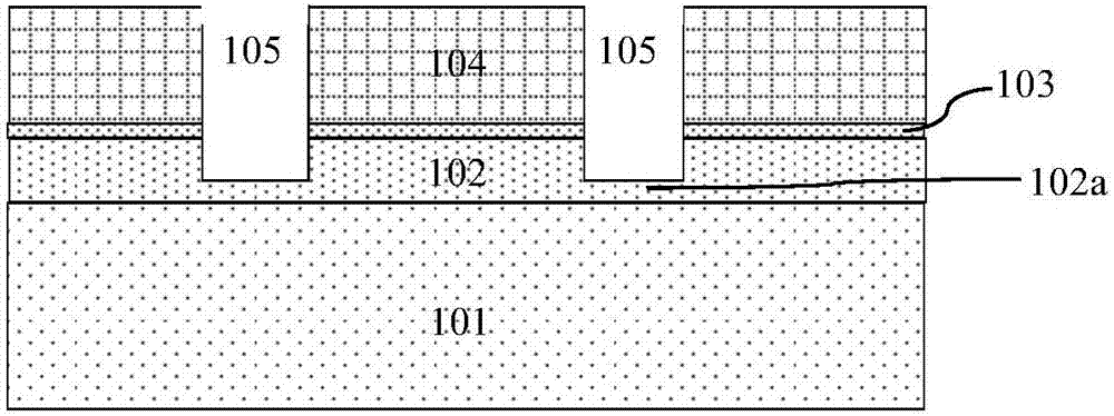
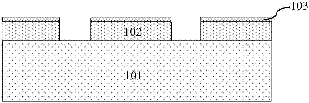
[0034] like figure 2 Shown is the flowchart of the manufacturing method of the SAB layer graphic structure of the embodiment of the present invention; Figure 3A to Figure 3C As shown, it is a device cross-sectional structure diagram in each step of the manufacturing method of the SAB layer graphic structure of the embodiment of the present invention, and the manufacturing method of the SAB layer graphic structure of the embodiment of the present invention includes the following steps:

[0035] Step 1, such as Figure 3A As shown, the SAB layer 2 is formed on the surface of the silicon substrate 1; the thickness of the SAB layer 2 is designed according to the thickness of the loss in the subsequent step 6 and is on the basis of satisfying the thickness of the metal silicide self-aligned mask Increase the thickness of the loss from step six.

[0036] Preferably, the material of the SAB layer 2 is silicon oxide.

[0037] Step two, such as Figure 3A As shown, a photoresist ...


PUM


Abstract

The invention discloses a manufacturing method of an SAB layer graph structure. The manufacturing method comprises the steps of 1, forming an SAB layer on the surface of a silicon substrate; 2, coating the surface of the SAB layer with photoresist; 3, performing photoetching to form a photoresist graph to define a metal silicide formation region; 4, by taking the photoresist graph as a mask, performing dry etching on the SAB layer, wherein the SAB layer formed in the metal silicide formation region is not fully removed by dry etching while a part of thickness is remained; 5, removing the photoresist graph in a condition that a part of thickness of the SAB layer is remained in the metal silicide formation region; and 6, completely removing the SAB layer remained in the metal silicide formation region by adopting a wet etching process to form the SAB layer graph structure. By virtue of manufacturing method, the technological cost can be lowered, photoresist striping can be prevented and application requirement can be satisfied.

Description

technical field [0001] The invention relates to a method for manufacturing a semiconductor integrated circuit, in particular to a method for manufacturing a metal silicide barrier layer (Salicide Block, SAB) layer pattern structure. Background technique [0002] In the semiconductor manufacturing process, there are two methods of SAB: one is to etch through dry and wet, and the other is to use pure wet etching. The common point of both is the use of i-line photoresist. And they all use glue to etch oxide; among them, the i-line light corresponds to a wavelength of 365nm. [0003] For small-scale processes, KRF glue must be used. KRF is expressed as krypton fluoride excimer laser with a wavelength of 248nm. KrF glue is the photoresist corresponding to 248nm laser. The higher the precision, the smaller the photolithography size can be made. In order to prevent photoresist peeling, stripping and adding a hard mask layer (Hardmask) are used to protect the underlying SAB layer,...

Claims


Application Information

Patent Timeline
IPC IPC(8): H01L21/033
CPCH01L21/0337
Inventor 沈冬冬王乐平隋建国
Owner SHANGHAI HUAHONG GRACE SEMICON MFG CORP
Features
  • R&D
  • Intellectual Property
  • Life Sciences
  • Materials
  • Tech Scout
  • Unparalleled Data Quality
  • Higher Quality Content
  • 60% Fewer Hallucinations
Learn More