Ultra-high-speed shutter semiconductor image sensor

An image sensor and semiconductor technology, which is applied in semiconductor devices, electric solid-state devices, radiation control devices, etc., can solve the problems of difficult sensor layers, and achieve the effects of improving time resolution, high shutter efficiency, and simplifying design

Active Publication Date: 2017-12-19
SHENZHEN UNIV
View PDF7 Cites 0 Cited by
  • Summary
  • Abstract
  • Description
  • Claims
  • Application Information

AI Technical Summary

Problems solved by technology

At the same time, it is very difficult to manufacture this sensor layer, and there is no report on the successful manufacture of this sensor layer.
Moreover, although the readout chip is based on a 0.18-micron CMOS process, its highest time resolution is only about 200 picoseconds

Method used


Image

  • Ultra-high-speed shutter semiconductor image sensor
  • Ultra-high-speed shutter semiconductor image sensor
  • Ultra-high-speed shutter semiconductor image sensor

Examples


Embodiment 1

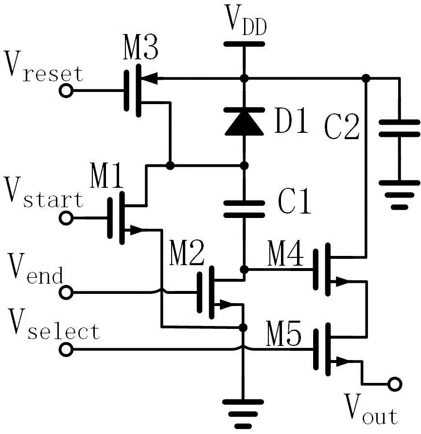
[0029] figure 1 It is an equivalent schematic diagram of the pixel unit circuit in this embodiment, wherein the photodiode D1 uses a p+ / n well photodiode, the side length of the p+ region is 7 microns, and the pixel pitch is 24 microns. Capacitor C1 is a signal storage capacitor, which is implemented using polysilicon-polysilicon capacitors. Capacitor C2 is a power supply decoupling capacitor, which uses a polysilicon gate-n+ capacitor, that is, a depletion-type NMOS transistor capacitor. M1 and M2 are respectively an exposure start control transistor and an exposure end control transistor, M3 is a reset transistor, and M4 and M5 form a readout buffer and selection circuit.

[0030] In this embodiment, the cross section of photodiode D1 is as follows figure 2shown. In order to fully shield stray light, especially for the drain of M2, except for an opening at the position of photodiode D1, other positions are covered by a light-shielding layer made of top metal. The edge o...

Embodiment 2

[0037] Example 1: The ultra-high shutter speed global shutter semiconductor image sensor realized by standard CMOS mixed-signal technology has excellent shutter efficiency only for short-wavelength visible light and ultraviolet light, but the residual sensitivity to 650nm red light is as high as 14,000 points one.

[0038] However, the ultra-high shutter speed global shutter semiconductor image sensor of this embodiment uses a triple-well CMOS mixed-signal process, and is realized by a deep n-well CMOS mixed-signal process including an isolated p-well. Among them, in figure 1 The equivalent schematic diagram of the pixel unit circuit shown, the exposure end control body port p-well of NMOS transistor M2 is a grounded isolated p-well in a deep n-well connected to a high potential, below which is a grounded p-well type substrate. The purpose of shielding the bulk port p-well of M2 with deep n-well isolation is to shield stray photogenerated carriers, thereby further improving ...

Embodiment 3

[0040] In Example 2, if the substrate-isolated p-well of the exposure end control transistor M2 is connected to a potential lower than the ground instead of the ground and the corresponding power supply decoupling capacitance is increased, although the dark current signal can also be reduced, the dark current is reduced to a limited extent and also has an impact on imaging sensor performance. At the same time, the power supply decoupling capacitor will occupy a large amount of chip area.

[0041] Figure 5 It is an equivalent schematic diagram of the pixel unit circuit in the third embodiment. The source of M2 is connected to the output of the CMOS inverter composed of transistors M6, M7, rather than directly connected to ground. M7 is an NMOS transistor with the shortest gate length and large gate width. When a few nanoseconds or more have elapsed since the exposure ends, V reset Turning to low level, the output terminal of the inverter composed of M6 and M7, that is, the...


PUM


Abstract

The invention discloses a semiconductor image sensor. A shading structure made of a non-transparent conductive material covers positions in a pixel array except for a photosensitive area of a photodiode (D1). The shading structure and an area which is made of a semiconductor material and forms one pole of the photodiode (D1) form annular contact. An opening is only arranged at a position of a lead wire which leads out another pole of the photodiode (D1). In the shading structure, each annular contact internal portion and the opening possess holes in the pixel array. In the invention, drain electrodes of exposure start and stop control transistors (M1 and M2) are connected to two ends of a signal storage capacitor (C1) respectively. When a 0.5 micron CMOS mixing signal technology is applied, shortest shutter gating time is only 75 picoseconds and residual sensitization to 405 nanometer visible light is as low as one in eighty million. Ultra-high-speed shutter and low residual sensitization characteristics are possessed.

Description

technical field [0001] The invention relates to a semiconductor image sensor, in particular to a semiconductor image sensor with an ultra-high-speed shutter. Background technique [0002] In the process of scientific research and technology development, it is often necessary to take continuous pictures with very short time intervals, that is, high-speed framing photography, for certain transient processes that cannot be accurately repeated. When the required time resolution is below nanoseconds, such high-speed framing photography usually needs to be realized by using high-speed photography equipment based on microchannel plate image intensifiers; when the required time resolution is several picoseconds to about thirty picoseconds, It needs to be realized with a microchannel plate image intensifier-based device combined with time stretching technology. Other high-speed framing techniques that achieve this time-resolved range include sequentially timed all-optical mapping ph...

Claims


Application Information

Patent Timeline
Patent Type & Authority Applications(China)
IPC IPC(8): H01L27/146
CPCH01L27/146H01L27/14601H01L27/14605H01L27/14643
Inventor 张帆牛憨笨
Owner SHENZHEN UNIV
Why Eureka
Try Eureka