
Fuse wire oxide layer etching method

A technology of oxide layer and fuse, which is applied in the manufacture of electrical components, electric solid devices, semiconductor/solid devices, etc., can solve problems such as fuse failure, circuit failure, and inability to precisely control the etching oxide layer, achieving low cost , Short time consumption, avoiding the effect of fuse blown failure

Inactive Publication Date: 2017-12-26
许斌
View PDF0 Cites 0 Cited by
  • Summary
  • Abstract
  • Description
  • Claims
  • Application Information

AI Technical Summary

Problems solved by technology

Fuses sometimes fail to blow, causing the entire circuit to fail
The traditional method of etching the oxide layer on both sides of the fuse structure cannot precisely control the amount of etched oxide layer

Method used


Image

  • Fuse wire oxide layer etching method

Examples


Embodiment Construction

[0013] The present invention will be further described below in conjunction with drawings and embodiments. It should be understood that the specific embodiments described here are only used to explain the present invention, but not to limit the present invention. In addition, it should be noted that, for the convenience of description, only some parts related to the present invention are shown in the accompanying drawings but not the whole content. Unless otherwise defined, all technical and scientific terms used herein are related to the technical field of the present invention. The skilled person generally understands the same meaning. The terms used herein are for describing specific embodiments only, and are not intended to limit the present invention.

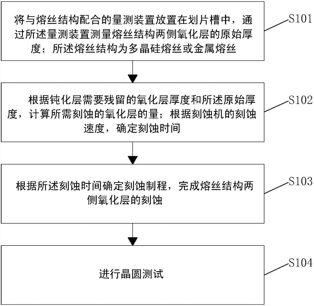
[0014] Please refer to figure 1 as shown, figure 1 A flow chart of a method for etching an oxide layer of a fuse provided in an embodiment of the present invention. The method for etching the oxide layer of the fuse in...


PUM


Abstract

The invention discloses a method for etching an oxide layer of a fuse, comprising: S101, placing a measuring device matched with a fuse structure in a scribing groove, and measuring the oxide layer on both sides of the fuse structure through the measuring device The original thickness; the fuse structure is a polysilicon fuse or a metal fuse; S102, according to the thickness of the oxide layer remaining in the passivation layer and the original thickness, calculate the amount of the oxide layer to be etched; according to the etching machine The etching speed is determined to determine the etching time; wherein, the material of the passivation layer is selected from silicon oxynitride; wherein, the etching machine adopts dry etching; S103, determine the etching process according to the etching time, The etching of the oxide layer on both sides of the fuse structure is completed; S104, performing a wafer test. The invention can precisely control the amount of oxide layer etched on both sides of the fuse structure, avoid the failure phenomenon of fuse blowing, and has low cost.

Description

technical field [0001] The invention relates to the technical field of semiconductors, in particular to a method for etching a fuse oxide layer. Background technique [0002] With the rapid development of integrated circuits, the manufacturing process of integrated circuits has become more and more complex and refined, and semiconductor components have become more susceptible to various defects, and the failure of a single component such as a transistor or a memory unit often causes lead to functional defects of the entire integrated circuit. The fuse structure is used to connect the redundant circuits in the integrated circuit. When the circuit is defective, the fuse is blown, so that the redundant circuit can repair or replace the defective circuit. The fuse structure is often used in memory. When the production of memory chips is completed, if some memory cells have functional problems, they can be replaced with redundant memory cells through the fuse structure to achiev...

Claims


Application Information

Patent Timeline
IPC IPC(8): H01L21/311H01L21/67H01L23/525
CPCH01L21/31116H01L21/67253H01L23/5256
Inventor 许斌
Owner 许斌
Learn More