Supercharge Your Innovation With Domain-Expert AI Agents!

A kind of LED encapsulation structure and encapsulation method thereof with double-layer phosphor layer

A technology of LED encapsulation and phosphor layer, applied in electrical components, circuits, semiconductor devices, etc., can solve the problems of uneven phosphor coating, decreased light output efficiency, and high processing cost, and achieve controllable light, heat reduction, packaging The effect of high processing efficiency

Active Publication Date: 2018-08-28
HAIDIKE NANTONG OPTOELECTRONICS TECH CO LTD
View PDF9 Cites 0 Cited by
  • Summary
  • Abstract
  • Description
  • Claims
  • Application Information

AI Technical Summary

Problems solved by technology

[0005] The phosphor is directly coated on the periphery of the chip, which means that the light emitted from the chip touches the phosphor. This light output mode has two disadvantages: 1. Part of the light is emitted from the side wall of the chip, which greatly reduces the light output efficiency
2. Due to the uneven coating of phosphor powder, there are differences in the emitted light, which requires further sorting, resulting in low yield and other shortcomings
[0006] In addition, the packaging of existing LEDs is generally prepared through the following steps: chip wafer cutting→split→test binning→sorting / arranging→CPS packaging→test binning→packaging. This packaging process requires two-step test binning. , resulting in low packaging efficiency and high processing costs

Method used


Image

  • A kind of LED encapsulation structure and encapsulation method thereof with double-layer phosphor layer

Examples


Embodiment 1

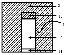
[0027] This embodiment has an LED packaging structure with double phosphor layers, such as figure 1 As shown, it includes a first package body 1 and a package adjustment phosphor layer 2 encapsulated on the top and side surfaces of the first package body; wherein, the first package body 1 includes LED chips 11 and substrate 12 arranged in sequence from bottom to top And phosphor layer 13.

Embodiment 2

[0029] Regarding the packaging method of the LED packaging structure with double phosphor layers of embodiment 1, the packaging method includes the following steps:

[0030] (1) First, perform WLP packaging, and coat a layer of phosphor on the back of the chip substrate after WLP packaging to form a phosphor layer 13 with a thickness of 10 µm-1000 µm;

[0031] (2) Cut the LED chip 11 coated with phosphor in step (1), and then use a splitting machine to split it from the dicing path until the split does not appear double crystals, forming the first package body 1;

[0032] (3) The first package 1 of step (2) is tested and binned, and the qualified first package 1 is sorted and arranged in accordance with the requirements of light and color separation according to brightness, display index and color temperature;

[0033] (4) Mix and stir the silica gel with a mass ratio of 97:3 and phosphor powder until no bubbles appear to form a regulated phosphor;

[0034] (5) Apply the first package b...

Embodiment 3

[0037] The packaging method of the LED packaging structure with double phosphor layers in this embodiment, wherein the LED chip 11 is a 820 chip, and the substrate 12 is a sapphire substrate. The specific packaging steps are as follows:

[0038] (1) First, perform WLP packaging, and coat a layer of phosphor on the back of the chip substrate after WLP packaging to form a phosphor layer 13 with a thickness of 100 µm;

[0039] (2) Cut the LED chip 11 coated with phosphor in step (1) to a size of 200 um×500 um, and then use a splitter to split from the dicing path until no double crystal appears in the split, forming the first package Body 1

[0040] (3) The first package body 1 in step (2) is tested and binned, and a single spot test is used, and the bins are divided according to different wavelength and brightness parameters. The qualified first package body 1 is based on the requirements of light and color separation. Sorting and arrangement of brightness, CRI and color temperature; ...


PUM


Abstract

The invention relates to an LED packaging structure having double phosphor layers and a packaging method thereof. The LED packaging structure comprises a first packaging body and a packaging and adjusting phosphor layer which is packaged on the top surface and the side surface of the first packaging body. The first packaging body comprises an LED chip, a substrate and the phosphor layers which arearranged from bottom to the top in turn. A layer of phosphor is directly coated on the back surface of the substrate firstly and then cutting, splitting, bin distribution test and sorting / arranging are performed, and then secondary phosphor coating and adjusting are performed according to the test result. The advantages of the LED packaging structure and the packaging method thereof are that theLED luminous efficiency is enabled to be higher and the light is enabled to be more uniform by the LED packaging structure; and the packaging method has high packaging efficiency and low processing cost.

Description

Technical field [0001] The invention belongs to LED packaging technology, and particularly relates to a double-layer phosphor layer [0002] LED packaging structure and packaging method thereof. Background technique [0003] LED is a solid-state semiconductor device that can directly convert electrical energy into light energy. It changed the principle of the three primary color powders of incandescent lamps, tungsten filaments and energy-saving lamps, and adopted electroluminescence. The characteristics of LED are very obvious, the main characteristics are long life, high luminous efficiency, low radiation and low power consumption. Almost all the spectrum of white light LED is concentrated in the visible light frequency band, and its luminous efficiency can exceed 150 lm / W. [0004] LED packaging refers to the packaging of light-emitting chips, which is quite different from integrated circuit packaging. The packaging of LEDs not only requires protection of the wick, but also li...

Claims


Application Information

Patent Timeline
Patent Type & Authority Patents(China)
IPC IPC(8): H01L33/00H01L33/48H01L33/50H01L33/64
Inventor 王南梁宗文杨刚孙智江
Owner HAIDIKE NANTONG OPTOELECTRONICS TECH CO LTD
Features
  • R&D
  • Intellectual Property
  • Life Sciences
  • Materials
  • Tech Scout
  • Unparalleled Data Quality
  • Higher Quality Content
  • 60% Fewer Hallucinations
Learn More