Integrated circuit (IC) package processing device and processing method

A technology for processing devices and packages, applied in the manufacture of electrical components, semiconductor/solid-state devices, circuits, etc., can solve the problems of long processing cycle, high cost, cumbersome control, etc., and achieve smooth control between processes, easy stripping, and optimization The effect of encapsulation process

Active Publication Date: 2018-01-19
深圳市鼎华芯泰科技有限公司
View PDF4 Cites 3 Cited by
  • Summary
  • Abstract
  • Description
  • Claims
  • Application Information

AI Technical Summary

Problems solved by technology

However, this requires repeated workpiece circulation between the packaging factory and the substrate factory, the processing cycle is long, and the control between processes is cumbersome; the corrosion of the carrier metal and the loss of precious metals lead to high costs

Method used


Image

  • Integrated circuit (IC) package processing device and processing method
  • Integrated circuit (IC) package processing device and processing method
  • Integrated circuit (IC) package processing device and processing method

Examples


Embodiment 1

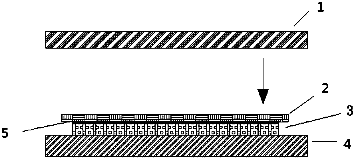
[0036] like figure 1 As shown, it shows a schematic diagram of the working state of the IC package processing device in this embodiment, and the device includes:

[0037] The first temperature-controlled suction cup 1 is used for adsorbing the metal carrier board 2 and heating the carrier board.

[0038] The second temperature control suction cup 4 is used for adsorbing the IC package body 3 and controlling the IC package body to be kept within the first temperature range.

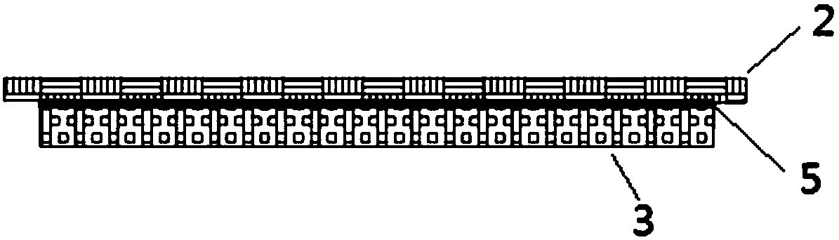
[0039] A separating device is used for starting when the temperature of the metal carrier is heated to a second temperature range by the first temperature-controlled suction cup, so as to separate the metal carrier and the IC package. In this embodiment, there is a low melting point metal plating layer 5 between the metal carrier 2 and the IC package 3 .

[0040] In this embodiment, the working process of the device includes: the IC package to be processed is sent into the processing device, such as fi...

Embodiment 2

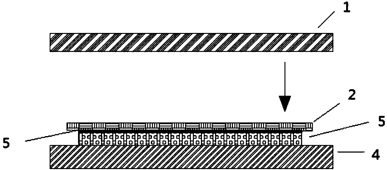
[0043] like figure 1 As shown, it shows a schematic diagram of the working state of the IC package processing device in this embodiment, and the device includes:

[0044] The first temperature-controlled suction cup 1 is used for adsorbing the metal carrier board 2 and heating the carrier board. In a specific device configuration, the suction cup may include a heating unit and an adsorption unit. The heating unit can adopt a non-contact heating method or a contact heating method.

[0045] In some instances, contact and non-contact heating units can also be used simultaneously to meet the requirements of different temperature control and heating modes.

[0046] In some examples, the non-contact heating unit includes a high frequency electromagnetic heating subunit.

[0047] In some examples, the contact heating unit includes at least one of an electrical heating subunit and a heat medium heating subunit.

[0048]In some examples, the adsorption unit of the first temperature...

Embodiment 3

[0055] like image 3 , 4 As shown, this embodiment discloses a method for post-processing the IC package, including the following steps:

[0056] Step 1. Inserting step: placing the non-metallic side of the IC package to be processed into the second temperature-controlled suction cup.

[0057] Specifically, the second temperature-controlled suction cup can be a vacuum adsorption suction cup, such as a porous negative pressure adsorption device. The porous negative pressure adsorption device can have a disk-shaped shape, and gas circulation pipes are distributed on its surface, and the pump device can be used to pump air to the outside through the gas circulation pipes, so as to realize negative pressure on the surface of the suction cup and the adsorbed object, so that the two are closely connected. connect.

[0058] There is a cooling medium inside the suction cup, and when the temperature exceeds a predetermined value, the temperature of the IC package absorbed by the sec...


PUM


Abstract

The invention proposes an integrated circuit (IC) package processing device and processing method. The structure comprises a first temperature control suction disc, a second temperature control suction disc and a separation control unit, wherein the first temperature control suction disc is used for absorbing a metal carrier plate and heating the carrier plate, the second temperature control suction disc is used for absorbing an IC package body and controlling the IC package body to be maintained within a first temperature range, and the separation control unit is used for separating the metalcarrier plate from the IC package body when a temperature of the metal carrier plate is heated to reach a second temperature range and is started by the first temperature control suction disc. By theIC package processing device, the package process is optimized, the cost is favorably reduced, green production is achieved, a workpiece is not needed to be repeatedly circulated between a package plant and a substrate plant, so that the processing period is shortened, and control among processes is smoother.

Description

technical field [0001] The invention belongs to the technical field of semiconductor device manufacturing, and in particular relates to an IC package processing device and a processing method. Background technique [0002] Quad Flat No-lead Package (QFN) technology is an important IC packaging process, with surface mount packaging, small pad size, small volume, small PCB area, thin component thickness, Very low impedance and self-inductance, which can meet the advantages of high-speed or microwave applications. The QFN has excellent electrical and thermal performance due to the large exposed pad in the bottom center being soldered to the thermal pad of the PCB. However, the disadvantage is that the middle part of the QFN is continuously wired around, the line width is limited by the copper thickness, and it is difficult to design island electrodes. The production cost and reliability problems caused by increasing the number of I / Os limit the design freedom of chips and PCB ...

Claims


Application Information

Patent Timeline
Patent Type & Authority Applications(China)
IPC IPC(8): H01L21/683
Inventor 何忠亮丁华徐光泽罗再成李亮叶文
Owner 深圳市鼎华芯泰科技有限公司
Why Eureka
Try Eureka