Flash memory unit structure forming method

A technology of flash memory cells and shallow trenches, applied in electrical components, electrical solid devices, circuits, etc., can solve the problems of charge loss, large influence at grain boundaries, and the sharp corners of floating gates cannot be rounded, etc., to achieve high Reliability, the effect of not damaging the floating gate

Inactive Publication Date: 2018-01-23
SHANGHAI HUALI MICROELECTRONICS CORP
View PDF6 Cites 0 Cited by
  • Summary
  • Abstract
  • Description
  • Claims
  • Application Information

AI Technical Summary

Problems solved by technology

[0005] Disadvantages: After silicon nitride is removed, the flash memory area is opened to remove silicon oxide, which affects the surface of the floating gate, and the uniformity of the surface oxidation becomes worse after removal (because the floating gate is polysilicon, the grain boundary has a greater impact)
[0008] Disadvantages: The sharp corners of the floating gate cannot be exposed because the silicon nitride has not been removed, resulting in the sharp corners of the floating gate not being rounded, and the subsequent high electric field is easy to accumulate, and there is a risk of charge loss
[0009] These two methods cannot simultaneously realize the rounding of the corners of the floating gate and the problem that the top of the floating gate of the flash memory is damaged by dry etching

Method used


Image

  • Flash memory unit structure forming method
  • Flash memory unit structure forming method
  • Flash memory unit structure forming method

Examples


Embodiment Construction

[0027] The specific embodiments of the present invention are given below in conjunction with the accompanying drawings, but the present invention is not limited to the following embodiments. Advantages and features of the present invention will be apparent from the following description and claims. It should be noted that all the drawings are in very simplified form and use imprecise ratios, which are only used for the purpose of conveniently and clearly assisting in describing the embodiments of the present invention.

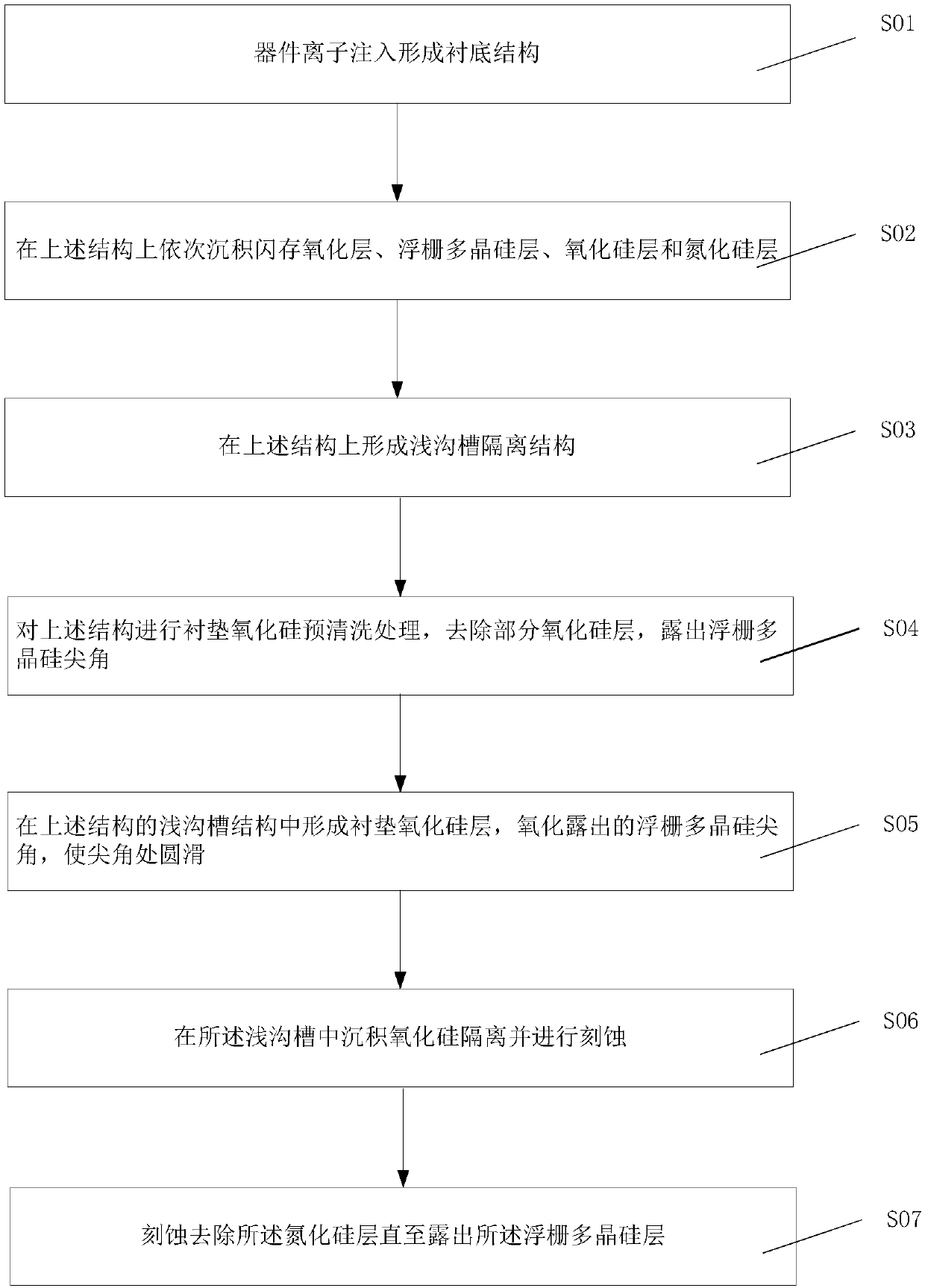
[0028] Please refer to figure 1 , figure 1 Shown is a flow chart of a method for forming a flash memory cell structure in a preferred embodiment of the present invention. The present invention proposes a method for forming a flash memory unit structure, comprising the following steps:

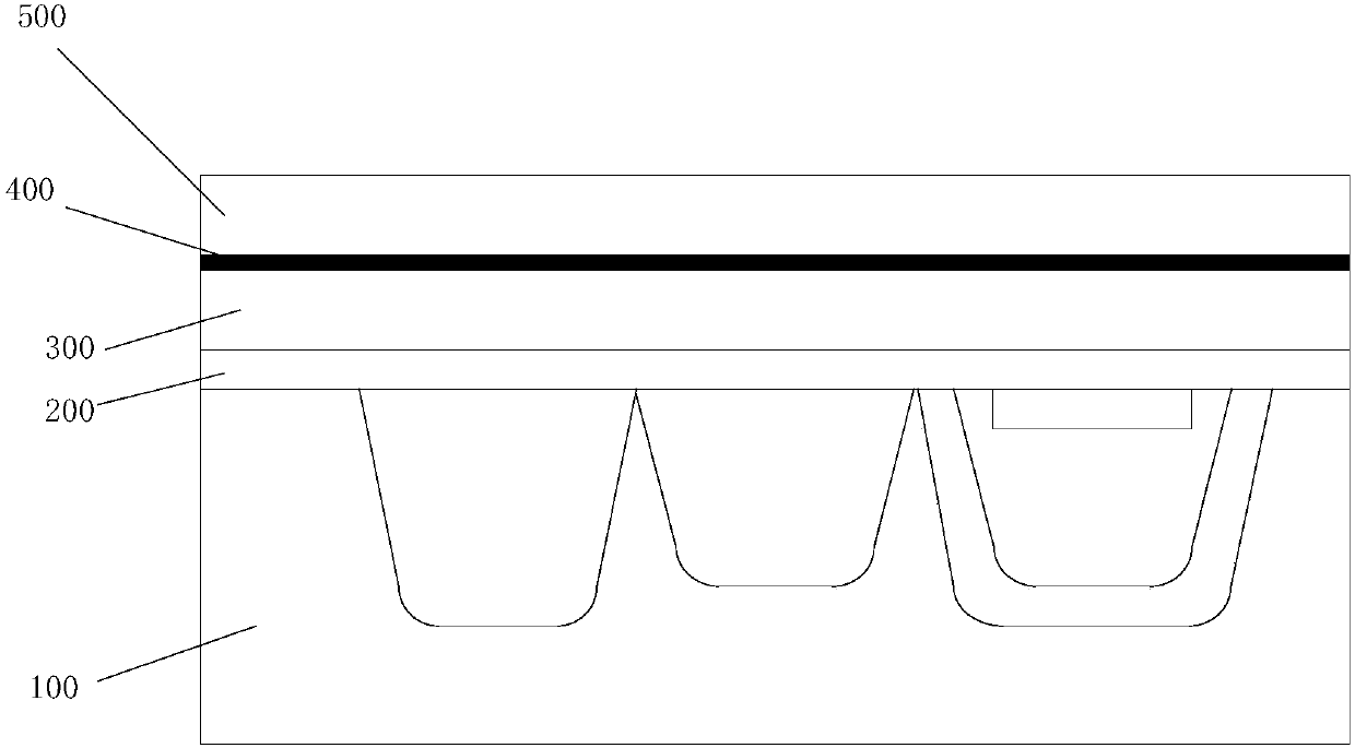
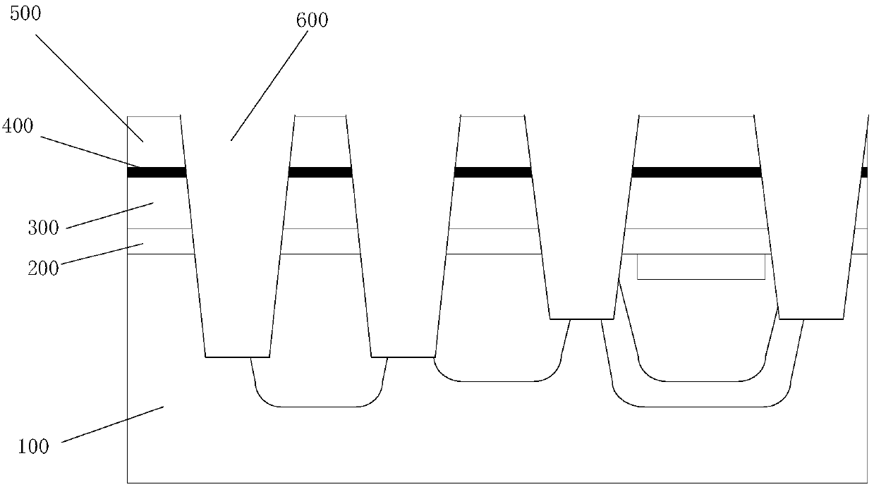
[0029] Step S01: device ion implantation to form a substrate structure;

[0030] Step S02: sequentially depositing a flash memory oxide layer, a floating gate polysilicon l...


PUM

PropertyMeasurementUnit
Thicknessaaaaaaaaaa

Abstract

The invention provides a flash memory unit structure forming method. The method comprises the following steps: device ion implantation is carried out to form a substrate structure; a flash memory oxide layer, a floating gate polysilicon layer, a silicon oxide layer and a silicon nitride layer are deposited sequentially on the above structure; a shallow trench isolation structure is formed on the above structure; liner silicon oxide pre-cleaning is carried out on the above structure, part of the silicon oxide layer is removed, and a floating gate polysilicon sharp point is exposed; a liner silicon oxide layer is formed in the shallow trench structure of the above structure, the exposed floating gate polysilicon sharp point is oxidized, and the sharp point is smooth; the silicon oxide isolation is deposited in the shallow trench and is etched; and the silicon nitride layer is etched and removed until the floating gate polysilicon layer is exposed. According to the flash memory unit structure forming method provided by the invention, the process integration problem of a 45-nanoscale flash memory unit is solved, and the flash memory unit with floating gate sharp point rounding and floating gate surface non damage can be acquired.

Description

technical field [0001] The invention relates to the field of semiconductor integrated circuit manufacturing, and in particular to a method for forming a flash memory unit structure. Background technique [0002] Flash memory has been widely used as the best choice for non-volatile memory applications due to its advantages of high density, low price, and electrical programmability and erasability. At present, flash memory cells are mainly implemented at the 65nm technology node. With the demand for large-capacity flash memory, the number of chips on each silicon wafer will be reduced by using the existing technology nodes. At the same time, the increasing maturity of new technology nodes also promotes the production of flash memory cells with high-node technologies. It means that the size of the flash memory unit needs to be reduced. The reduction of the active area width and channel length of the flash memory unit according to the original structure will affect the mutual i...

Claims


Application Information

Patent Timeline
IPC IPC(8): H01L27/11521H01L27/11548
Inventor 田志钟林建殷冠华陈昊瑜
Owner SHANGHAI HUALI MICROELECTRONICS CORP
Why Eureka
Try Eureka