Broadband ultrahigh frequency electronic label and manufacturing method thereof

An electronic label and ultra-high frequency technology, which is applied to record carriers, instruments, computer parts, etc. used in machines, can solve problems such as fracture failure and antenna pattern damage, and achieve the effect of prolonging life, improving efficiency and satisfying impedance matching.

Inactive Publication Date: 2018-01-26
BEIJING YISIDE LOGISTICS TECH
View PDF0 Cites 2 Cited by
  • Summary
  • Abstract
  • Description
  • Claims
  • Application Information

AI Technical Summary

Problems solved by technology

Due to the large deflection and elongation of the base, the antenna pattern will be damage

Method used


Image

  • Broadband ultrahigh frequency electronic label and manufacturing method thereof
  • Broadband ultrahigh frequency electronic label and manufacturing method thereof
  • Broadband ultrahigh frequency electronic label and manufacturing method thereof

Examples


Embodiment 1

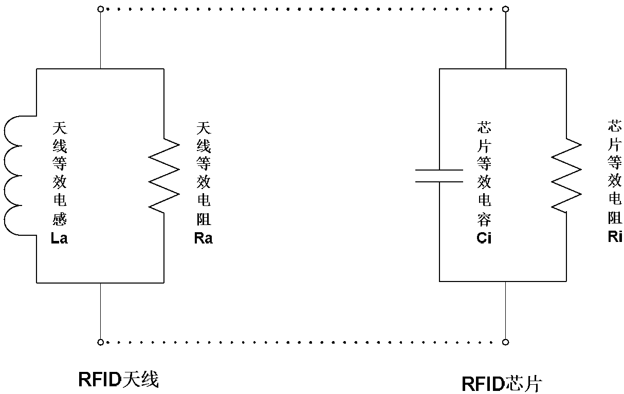
[0042] When the impedance conjugates of the antenna and the tag correspond to each other, the UHF RFID tag achieves the best impedance matching; the impedance conjugate relationship between the tag antenna and the tag chip is as follows:

[0043] Z ANT = R ANT +j*X ANT

[0044] Z IC = R IC +j*X IC

[0045] R ANT = R IC

[0046] x ANT =-X IC

[0047] Taking the chip NXP-G2XM as an example, the equivalent circuit diagram of the chip NXP-G2XM can be found in the attached figure 2 , assuming that the value of its parallel resistance Ri is equal to X, and the value of its parallel capacitance Ci is equal to XpF. The ADS software is used to calculate the tag chip impedance. See attached Figure 6 a and attached Figure 6 b, which are the real and imaginary parts of the impedance of the chip as a function of frequency. According to the simulation data and analysis of ADS, according to the requirements of impedance conjugation, the real part of the antenna impedance ...

Embodiment 2

[0058] The electronic tag also needs to have a higher gain to transmit the maximum signal to the chip in the electronic tag, so as to provide a better communication effect for the chip. However, in actual use, electronic tags are often used in conjunction with corrugated packaging boxes. Due to the dielectric constant of the corrugated packaging box, the traditional UHF electronic tag has a large difference between the power of writing data and the power of reading data, which has caused the technical problem of the decline in the communication performance of the electronic tag. Based on the antenna structure in the present invention, the dielectric constant of the corrugated box is considered. Further, the antenna of the electronic tag is improved in detail.

[0059] The antenna structure in this embodiment is the same as the antenna structure in Embodiment 1, and the specific size design is as follows:

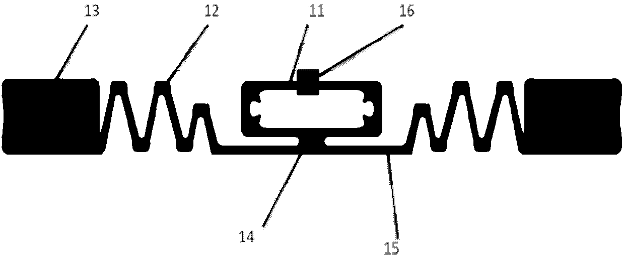
[0060] The closed stub ring 11 has a substantially rectangular outer ...

Embodiment 3

[0065] The antenna in embodiment 1 or embodiment 2 is usually arranged on an organic polymer material or a paper substrate, the material of the antenna is aluminum or copper, and the electronic chip is arranged on it and electrically coupled thereto. The inflection point of the V-shaped structure of the antenna in Embodiments 1 and 2 is a stress concentration area in the entire pattern structure. Because the base has a large deflection and extension, it will be in use due to the excessive bending and bending of the base. Excessive stretching will cause excessive stress at the bending point of the V-shaped structure of the antenna pattern in Embodiments 1 and 2, thereby causing breakage at this position.

[0066] Therefore, in this third embodiment, on the basis of the electronic tags in embodiments 1 and 2, a connecting portion 17 is provided at the bending point of the V-shaped structure of the antenna pattern. Considering the cost of materials and the impact on the antenna r...


PUM

PropertyMeasurementUnit
Angleaaaaaaaaaa
Lengthaaaaaaaaaa
Thicknessaaaaaaaaaa

Abstract

The invention relates to a broadband ultrahigh frequency electronic label. The broadband ultrahigh frequency electronic label comprises a chip and antenna portion, wherein the antenna portion comprises a short cut ring, two bending radiators and two radiation arrays, the short cut ring is a rectangular ring structure, one ends of the two bending radiators are connected with the short cut ring, theother ends of the two bending radiators are connected with the two radiation arrays, the two bending radiators are multiple bending portions composed of multiple V-shaped structures with different heights, the two radiation arrays are arranged at the outer-most side of the antenna portion, the vertical dimension of each radiation array is not smaller than the vertical dimension of the bending radiator, the transverse dimension is greater than the transverse dimension of the single V-shaped structure, and the short cut ring is connected with a ground end and a radio frequency end of a radio frequency chip and is further taken as a feed end of the label antenna. The electronic label is advantaged in that difference of writing data power and reading data power is reduced, impedance matchingis realized, signal gain is improved, miniaturization is realized, and mechanical performance and service life are further improved.

Description

technical field [0001] The invention relates to an electronic tag, in particular to a wide-band ultra-high frequency electronic tag and a manufacturing method thereof. Background technique [0002] as attached figure 1 As shown, the working principle of the electronic tag is that the reader 3 sends a radio frequency signal of a certain frequency through the transmitting antenna 2, and when the radio frequency tag 1 enters the working area of ​​the transmitting antenna, an induced current is generated, and the radio frequency tag 1 obtains energy and is activated; the radio frequency tag 1 will The information such as its own code is sent out through the transmitting antenna 2 built in the tag; the receiving antenna 2 of the system receives the carrier signal sent from the radio frequency tag, and transmits it to the reader-writer 3 through the antenna regulator; the reader-writer 3 decodes the received signal It is reconciled and decoded, and then sent to the computer syste...

Claims


Application Information

Patent Timeline
IPC IPC(8): G06K19/077
Inventor 常江
Owner BEIJING YISIDE LOGISTICS TECH
Why Eureka
Try Eureka